
“Bare Metal” STM32 Programming (Part 12): Using Quad-SPI Flash Memory
If I had to guess what the world’s most popular footprint for low-density memory chips was, I would probably be wrong. But I’ll bet that the humble 8-pin SOIC / DIP / DFN formats would be near the top. You’ve probably used these before; most ESP8266 and ESP32 modules have one under their little metal shield, and motherboards for computers / cars / synthesizers / etc. often use them for storing UEFI / BIOS / firmware configurations and suchlike.
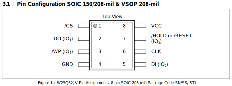
Pin assignments for a generic Flash module (Winbond W25Q series)
You can get RAM, Flash, EEPROM, and even FRAM memory in these common 8-pin packages. They usually use a SPI interface for communication, with a couple of extra pins for functions like write protection or suspending an ongoing transaction. But if you look in the image above, you’ll see that the /WP “Write Protect” and /HOLD or /RESET wires are also marked as IO2 and IO3. That’s because many 8-pin Flash chips also support a “Quad-SPI” interface, which is very similar to a bidirectional “3-wire” SPI interface, except that it has four I/O wires instead of one.
Some STM32 chips include a QSPI peripheral to interface with these kinds of Flash memory chips. You can use it to manually configure / erase / program the Flash chip, and once it’s initialized, you can also map the external Flash as read-only memory in the STM32’s internal memory space. The peripheral supports prefetching, caching, executing code, and it can even access two QSPI Flash chips in parallel, using 8 data lines in total to transfer a full byte of data every clock cycle.
To learn about the QSPI peripheral, I used the same STM32F723E Discovery Kit from my last post about external memories. In addition to its external RAM and display, this board includes one 64MB QSPI Flash chip connected to the QSPI peripheral. In this post, we’ll learn how to configure the Flash chip for quad I/O access, erase a sector, and write some test values. Then we’ll set the QSPI peripheral to its read-only “memory-mapped” mode, and read those test values by accessing the chip’s internal memory space starting at 0x90000000. If you don’t like copy/pasting, you can find an example project with this code on GitHub.
It is a little bit annoying that you can’t write to the Flash chip in memory-mapped mode, but this peripheral still presents a simple way to quickly read from external Flash using only six I/O pins. And writing to Flash memory has some unique limitations anyways, which is why it is often used to store data which an application rarely needs to modify, like firmware or audio/visual resources. So if you want to learn how to use Quad-SPI Flash memories with an STM32, read on!
“Bare Metal” STM32 Programming (Part 11): Using External Memories
Modern microcontrollers are amazing. They are much faster and cheaper than the sort of processors that powered “real” computers a few decades ago, and they’re also very power-efficient. But software complexity has also grown over time, and as we humans often say about ourselves as we age, it has grown in the wrong direction. Developers have gotten used to having enormous reserves of memory to draw from, so unless an application or library was specifically written for embedded platforms, it probably won’t be able to run with the scant kilobytes of RAM which are included in your average microcontroller.
Fortunately, most vendors include peripherals for accessing external memory when it is needed, and the STM32’s “Flexible Memory Controller” is surprisingly easy to use. Unfortunately, it is not easy to design a custom PCB with parallel memory modules. The interfaces use a lot of signals which are susceptible to electromagnetic noise, so it is important to ensure that all of the traces have the same length and impedance. This is especially hard on hobbyists, because 2-layer boards are not appropriate for these sorts of designs and KiCAD does not support length-matching for more than two traces yet.
So the target hardware for this tutorial will be a $40 STM32F723E Discovery Kit. It is a bit more expensive than the minimal “Nucleo” boards, but it includes 512KB of external RAM and a 240×240-pixel TFT display; we’ll learn how to drive both of those from the FMC peripheral in this post. It also includes 64MB of memory-mapped QSPI Flash memory, which I’ll talk about in a future post.
We’ll use the external RAM to store a framebuffer, which will be sent to the display using DMA.
This evaluation board uses BGA parts, which are almost impossible to solder without special equipment. But it provides an easy and affordable way to learn about writing software for these peripherals. When you are ready to use external memories in homemade designs, you can use QFP STM32s with at least 144 pins, TSSOP memory chips, and a 4-layer PCB.
Learning FPGA Design with nMigen
Like many of us, I’ve been stuck indoors without much to do for the past month or so. Unfortunately, I’m also in the process of moving, so I don’t know anyone in the local area and most of my ‘maker’ equipment is in storage. But there’s not much point in sulking for N months straight, so I’ve been looking at this as an opportunity to learn about designing and implementing FPGA circuits.
I tried getting into Verilog a little while ago, but that didn’t go too well. I did manage to write a simple WS2812B “NeoPixel” driver, but it was clunky and I got bored soon after. In my defense, Verilog and VHDL are not exactly user-friendly or easy to learn. They can do amazing things in the hands of people who know how to use them, but they also have a steep learning curve.
Luckily for us novices, open-source FPGA development tools have advanced in leaps and bounds over the past few years. The yosys and nextpnr projects have provided free and (mostly) vendor-agnostic tools to build designs for real hardware. And a handful of high-level code generators have also emerged to do the heavy lifting of generating Verilog or VHDL code from more user-friendly languages. Examples of those include the SpinalHDL Scala libraries, and the nMigen Python libraries which I’ll be talking about in this post.
I’ve been using nMigen to write a simple RISC-V microcontroller over the past couple of months, mostly as a learning exercise. But I also like the idea of using an open-source MCU for smaller projects where I would currently use something like an STM32 or MSP430. And most importantly, I really want some dedicated peripherals for driving cheap addressable “NeoPixel” LEDs; I’m tired of needing to mis-use a SPI peripheral or write carefully-timed assembly code which cannot run while interrupts are active.
But that will have to wait for a follow-up post; for now, I’m going to talk about some simpler tasks to introduce nMigen. In this post, we will learn how to read “program data” from the SPI Flash chip on an iCE40 FPGA board, and how to use that data to light up the on-board LEDs in programmable patterns.
The LEDs on these boards are very bright, because you’re supposed to use PWM to drive them.
The target hardware will be an iCE40UP5K-SG48 chip, but nMigen is cross-platform so it should be easy to adapt this code for other FPGAs. If you want to follow along, you can find a 48-pin iCE40UP5K on an $8-20 “Upduino” board or a $50 Lattice evaluation board. If you get an “Upduino”, be careful not to mis-configure the SPI Flash pins; theoretically, you could effectively brick the board if you made it impossible to communicate with the Flash chip. The Lattice evaluation board has jumpers which you could unplug to recover if that happens, but I don’t think that the code presented here should cause those sorts of problems. I haven’t managed to brick anything yet, knock on wood…
Be aware that the Upduino v1 board is cheaper because it does not include the FT2232 USB/SPI chip which the toolchain expects to communicate with, so if you decide to use that option, you’ll need to know how to manually write a binary file to SPI Flash in lieu of the iceprog commands listed later in this post.
Festive Cross-Platform Holiday Lights
Across the globe, people seem to enjoy decorating their homes, communities, and outdoor spaces with lights and ornaments during the winter holidays. Maybe it helps with the depressingly early sunsets for those of us who don’t live near the equator. Anyways, I thought it’d be fun to make some ornaments with multi-color addressable LEDs last year, and I figured I’d write about what worked and what didn’t.
I didn’t have many microcontrollers at the time because I was visiting family for the holidays, so I ended up coding the lighting patterns for a cheap little STM32F103 “black pill” board which was in the bottom of my backpack. And it’s a convenient coincidence that I just started learning about the very similar GD32VF103 chips with their fancy RISC-V CPUs and nearly-identical peripheral layout, so this also seems like a good opportunity to write about how to cross-compile the same code for two different CPU architectures.

Pretty holiday stars! “Frosted white” acrylic sheets aren’t the best way to diffuse light, but they are cheap and easy to work with.
This was a fun and festive project, and it might not be a bad way to introduce people to embedded development since there are so many ways to drive these ubiquitous “NeoPixel” LEDs. Sorry that this post is a little bit late for the winter holidays – I’ve been traveling for the past few months – but maybe it’ll get you thinking about next year 🙂
I’ll talk about how I assembled the stars and what I might do differently next time, then I’ll review how to light them up with an STM32F103, and how to adapt that code for a GD32VF103. But you could also use a MicroPython or Arduino board to set the LED colors if you don’t want to muck around with peripheral registers.
Bare-metal RISC-V Development with the GD32VF103CB
For the past few years, there has been growing excitement about the RISC-V instruction set architecture. It is an appealing architecture because it is open-source (which can mean royalty-free), and flexible enough to be configured for everything from small power-efficient microcontrollers to fast and complex application processors. In this post, we’ll learn how to write a simple program for a GigaDevice GD32VF103 chip, which leans towards the “small and power-efficient” end of the spectrum.
There have already been a handful of opportunities for hobbyists to use RISC-V hardware in their projects, such as the SiFive “Freedom” chips and Kendryte K210 modules. But the SiFive boards are expensive and (up until this point) produced in limited quantities, and most of the cheaper options have been narrowly focused on niches like machine learning or IoT applications. The GD32VF103 is still fairly new, and while there’s no guarantee that it won’t end up in history’s dustbin of one-off chips, it is an affordable general-purpose chip with a few tricks up its sleeve which should make it a nice learning platform.
First, it is easy to buy a handful of boards which use these chips: you can buy “Longan Nano” boards for about $5 from Seeed Studios, and they also sell compatible USB/JTAG debugging dongles. The GD32V chips have decent support for flashing and debugging, with a fork of DFU-utils to upload code over USB and a fork of OpenOCD to open a debugging connection to the chip. I hope that support for these chips is eventually integrated into the core projects, but in these early days, you’ll have to build patched versions.
There is also a HAL repository with C code to help you access the chip’s peripherals, but one more reason why this chip is an appealing learning platform is that its peripherals work very similarly to those found in the venerable STM32F1 family of microcontrollers. So while you can use the vendor-provided HAL, you can also get a head start on writing your own drivers by migrating code written for older STM32F103 chips, even though they have a different CPU architecture! How cool is that? 🙂
If any of that sounds interesting, keep reading – we’ll use the “Longan Nano” board that I mentioned above as the target hardware for this blog post, but the first few sections should apply to most boards that use a GD32VF103 chip. We’ll start with the basic boot/startup code which is needed to get to the ‘main’ method in a C program, then we’ll configure a few GPIO pins to toggle the on-board RGB LEDs. After that, we’ll set up a hardware interrupt to generate timed delays using the CPU’s timer peripheral (similar to ARM’s SysTick). Finally, we’ll set up DMA with the SPI peripheral to draw to the board’s 160×80-pixel display.
We’ll write some basic startup code for the chip, then set up its GPIO and SPI peripherals to light up the on-board LEDs and display.
Designing a Simple GPS Handheld
I’ve written a little bit in the past about how to design a basic STM32 breakout board, and how to write simple software that runs on these kinds of microcontrollers. But let’s be honest: there’s still a bit of a gap between creating a small breakout board to blink an LED, and building hardware / software for a ‘real-world’ application. Personally, I would still want a couple of more experienced engineers to double-check any designs that I wanted to be reliable enough for other people to use, but building more complex applications is a great way to help yourself learn.
So in this post, I’m going to walk through the process of designing a small ‘gameboy’-style handheld with a GPS receiver and microSD card slot, for exploring the outdoors instead of video games. Don’t get me wrong, you could still write games to run on this if you wanted to, and that would be fun, but everyone and their dog has made a Cortex-M-based handheld game console by now; there are plenty of better guides for that, and many of those authors put a lot more time into their designs and firmware than I ever did.
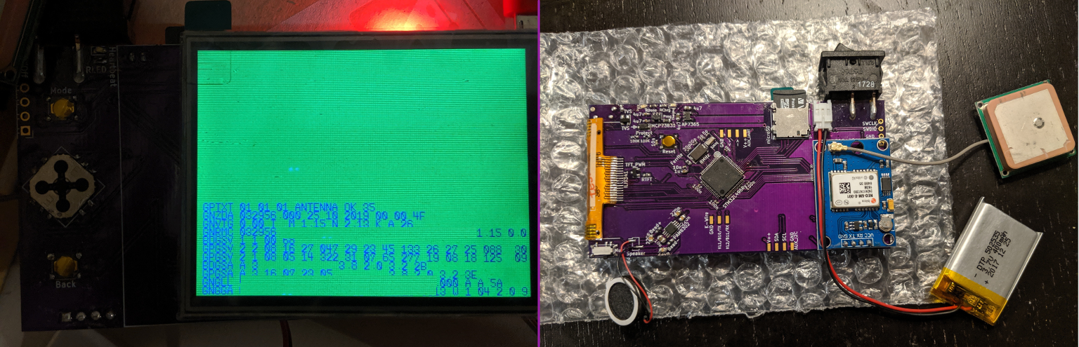
Assembled GPS Doohicky. I left too much room between the ribbon connector footprint and the edge of the board on this first revision, so the display couldn’t fold over quite right. Oh well, you live and learn.
The board design isn’t too complicated, but there are several different parts and it gets easier to make small-but-important mistakes as a design gets larger. It mostly uses peripherals that I’ve talked about previously, but there are a couple of new ones too. The display will be driven over SPI, the speaker uses a DAC, the GPS receiver talks over UART, the battery and light levels will be read using an ADC, and the buttons will be listened to using interrupts. But I haven’t written about the USB or SD card (“MMC”) peripherals, and those will need to go in a future post since I haven’t actually worked them out myself yet. Note that SD cards can technically use either SPI or SD/MMC to communicate, but the microcontroller that I picked has a dedicated SD/MMC peripheral, and I wanted to learn about it.
Anyways, if that sounds interesting, read on and let’s get started!
Simple USB / Serial Communication with the CP2102N
Several years ago, a company called Future Technology Devices International (FTDI) sold what may have been the most popular USB / Serial converter on the market at the time, called the FT232R. But this post is not about the FT232R, because that chip is now known for its sordid history. Year after year, FTDI enjoyed their successful chip’s market position – some would say that they rested too long on their laurels without innovating or reducing prices. Eventually, small microcontrollers advanced to the point where it was possible to program a cheap MCU to identify itself as an FT232R chip and do the same work, so a number of manufacturers with questionable ethics did just that. FTDI took issue with the blatant counterfeiting, but they were unable to resolve their dispute through the legal system to their satisfaction, possibly because most of the counterfeiters were overseas and difficult to definitively trace down. Eventually, they had the bright idea of publishing a driver update which caused the counterfeit chips to stop working when they were plugged into a machine with the newest drivers.
FTDI may have technically been within their rights to do that, but it turned out to be a mistake as far as the market was concerned – as a business case study, this shows why you should not target your customers in retaliation for the actions of a 3rd party. Not many of FTDI’s customers were aware that they had counterfeit chips in their supply lines – many companies don’t even do their own purchasing of individual components – so companies around the world started to get unexpected angry calls from customers whose toy/media device/etc mysteriously stopped working after being plugged into a Windows machine. You might say that this (and the ensuing returns) left a bad taste in their mouths, so while FTDI has since recanted, a large vacuum opened up in the USB / Serial converter market almost overnight.
Okay, that might be a bit of a dramatized and biased take, but I don’t like it when companies abuse their market positions. Chips like the CH340 and CH330 were already entering the low end of the market with ultra-affordable and easy-to-assemble solutions, but I haven’t seen them much outside of Chinese boards, possibly due to a lack of multilingual documentation or availability from Western distributors. So at least in the US, the most popular successor to the FT232R seems to have been Silicon Labs’ CP2102N.
It’s nice to have a cheap-and-cheerful way to put a USB plug which speaks UART onto your microcontroller boards, so in this post, I’ll review how to make a simple USB / UART converter using the CP2102N. The chip comes in 20-, 24-, and 28-pin variants – I’ll use the 24-pin one because it’s smaller than the 28-pin one and the 20-pin one looks like it has some weird corner pads that might be hard to solder. We’ll end up with a simple, small board that you can plug into a USB port to talk UART:
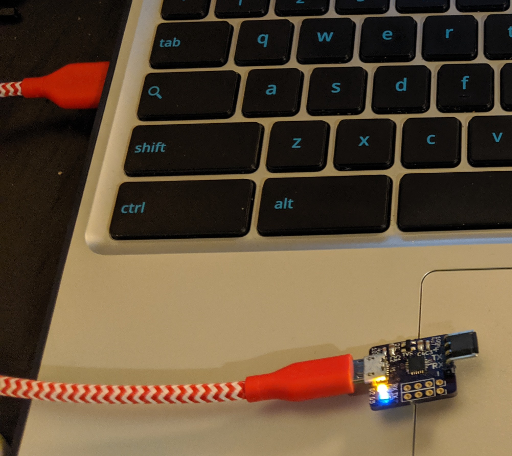
Drivers for the CP2102N are included in most popular OSes these days, including Linux distributions, so it’s mostly plug-and-play.
It’s worth noting that you can buy minimal CP2102N boards from AliExpress or TaoBao for about $1, but where’s the fun in that?
Reading Battery Voltage with the STM32’s ADC
If you choose to pursue embedded development beyond the occasional toy project, it probably won’t take long before you want to design something which runs off of battery power. Many types of devices would not be useful if they had to be plugged into a wall outlet all the time, and power efficiency is one of the biggest advantages that microcontrollers still have over application processors like the one in a Raspberry Pi.
When you do move an application to battery power, you’ll quickly discover that it is very important for your device to be able to A) charge its battery and B) alert you when its battery is running low. Not knowing whether something has hours or seconds of life left can be really annoying, and trying to use a nearly-dead battery can cause strange behavior, especially if the battery’s power drops off slowly as it dies. Most lithium-based batteries also last longer if you avoid fully discharging them – there’s some good information about lithium battery aging in this article.
So in this post, I’m going to go over a very basic circuit to power an STM32 board off of a single lithium-ion battery and monitor its state of charge. I will also talk briefly about how to add a simple battery charger to your design, but you should always independently verify any circuitry which interacts with lithium batteries! This circuit seems to work to the best of my knowledge, but don’t take my word for it; it’s very important to double- and triple-check your li-po battery circuits, because they can easily become serious fire hazards if they are handled improperly. It’s also good practice to avoid leaving lithium-ion batteries unattended while they are charging, and you should try to get batteries with built-in protection circuitry to help mitigate bad situations like over-current, under-voltage, etc.
So with those brief and not comprehensive safety warnings out of the way, let’s get started! I’ll use an STM32L4 chip for this example, but the ADC peripheral doesn’t seem to change much across STM32s. And here is a GitHub repository containing design files for a simple board which demonstrates the concepts described in this post.
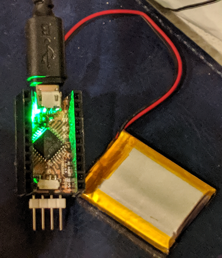
Hooray, it’s fully charged!
New 8-pin ARM Core: the STM32G031J6
It has been about nine months since ST released their new STM32G0 line of microcontrollers to ordinary people like us, and recently they released some new chips in the same linup. It sounds like ST wants this new line of chips to compete with smaller 8-bit micros such as Microchip’s venerable AVR cores, and for that market, their first round of STM32G071xB chips might be too expensive and/or too difficult to assemble on circuit boards with low dimensional tolerances.
Previously, your best bet for an STM32 to run a low-cost / low-complexity application was probably one of the cheaper STM32F0 or STM32L0 chips, which are offered in 16- and 20-pin TSSOP packages with pins spaced 0.65mm apart. They work great, but they can be difficult to use for rapid prototyping. It’s hard to mill or etch your own circuit board with tight enough tolerances, and it’s not very easy to solder the chips by hand. Plus, the aging STM32F031F6 still costs $0.80 each at quantities of more than 10,000 or so, and that’s pretty expensive for the ultra-cheap microcontroller market.
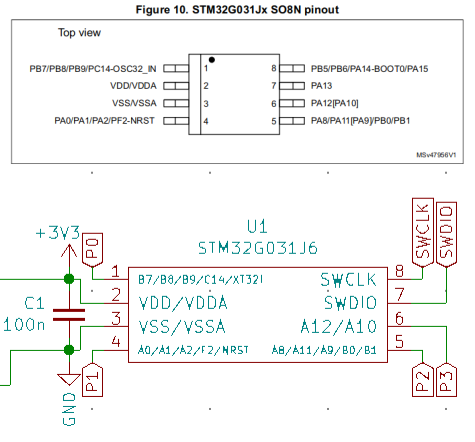
Pinout and minimal circuit for an STM32G031J6 – you only really need one capacitor if you have a stable 3.3V source.
Enter the STM32G031J6: an STM32 chip which comes in a standard SOIC-8 package with 32KB Flash, 8KB RAM, a 64MHz speed limit, and a $0.60 bulk price tag (closer to $1.20-1.40 each if you’re only buying a few). That all compares favorably to small 8-pin AVR chips, and it looks like they might also use a bit less power at the same clock speeds. Power consumption is a tricky topic because it can vary a lot depending on things like how your application uses the chip’s peripherals or what voltage the chip runs off of. But the STM32G0 series claims to use less than 100uA/MHz, and that is significantly less than the 300uA/MHz indicated in the ATTiny datasheets. Also, these are 32-bit chips, so they have a larger address space and they can process more data per instruction than an 8-bit chip can.
Considering how easy STM32 chips are to work with, it seems like a no-brainer, right? So let’s see how easy it is to get set up with one of these chips and blink an LED.
Mounting Solar Panels to a Car
As someone who likes both electronics and the outdoors, sometimes I get anxiety about a lack of electricity. It would be nice to go camping somewhere away from it all, and still be able to charge things and run some lights, a display, maybe a small cooler. I’m sure some of you are rolling your eyes at that, but I’ve also been wanting to play with adding aftermarket indicators to old cars, like backup sensors or blind spot warnings, and it’d be nice to run them off a separate battery to avoid the possibility of accidentally draining the car’s battery overnight.
Since low-power solar panels are fairly cheap these days, I figured that it might be worth buying a few to mount to my car’s roof. And since my car is technically a pickup, it was very easy to put the battery in the bed and run the wiring through the canopy’s front window:

I’ve secured the battery a bit more since taking these pictures, but this is the basic idea – it’s pretty simple.
If you have a different kind of car, I’d imagine that you could just as easily put the battery in your trunk, but you might need to drill a hole for the wires if you don’t want to leave one of your windows cracked open.
I guess that a lot of this guide won’t apply exactly to your situation, because you’ll have different dimensions to work with, different limitations, and probably different solar panels. But I hope that laying out each step that I took and what worked for me might be helpful – your basic approach could probably look very similar.
And before we go any further, please keep your expectations in check. These panels can only produce up to 100W in direct sunlight, which is nowhere near enough power for something like an electric vehicle. So read on if this sounds interesting, but the car still runs on gas. We’re not saving the world here.