
The past few months have been very trying, even for those of us who have been fortunate enough to remain healthy. It’s hard to find meaning when you can’t create things or do stuff for other people, and it’s hard to do either of those things when you don’t have access to tools, space to work in, or people to talk with. But sometimes, the only thing you can change about a situation is how you react to it. And it’s still possible to learn a lot with a few small circuit boards, even when you’re confined to a small apartment and everything is closed.
So in this post, I’m going to walk through the design of a simple RISC-V CPU using the Python-based nMigen HDL. It will run GCC-compiled code for the RV32I architecture, fit in an affordable iCE40UP5K FPGA with a bit of room to spare, and include a basic peripheral bus with simple GPIO. But it will also be pretty slow with a 12MHz top speed, and it won’t strictly conform to the RISC-V specification. Not all of the RV32I machine-mode features are necessary for a small microcontroller core, and space will be at a premium, so I decided to omit some irrelevant features to simplify the design. And some useful features like peripheral interrupts and JTAG debugging are also out-of-scope for this post, which is already sort of long and complicated.
I wrote a bit about nMigen previously, so check that article if you aren’t familiar with the library’s basic syntax and build / test / run process. And keep in mind that I’m not very experienced in digital design, so the code presented here probably won’t be optimal and it might include some poor design decisions. Suggestions and comments are very welcome, as always!
I’ll walk through the design of each basic CPU module in order, then how to simulate and run code on the resulting design:
- ISA: a file containing named definitions for the
RV32Iinstruction set’s opcodes, register addresses, etc. - ALU: the Arithmetic and Logic Unit performs the math operations which underlie individual instructions.
- Memories: the RAM and ROM modules, along with an interface to map them to different memory spaces.
- CSRs: logic to handle supported Control and Status Registers.
- CPU: logic which performs the processor’s core “read, decode, execute” logic.
- Tests: simulate the
RISC-Vcompliance tests, and other compiled C programs. - Peripherals: GPIO, PWM, and a multiplexer to choose which peripherals are assigned to which pins.
- Code: build and run example programs to toggle the on-board LEDs and pulse them using PWM.
So if you are interested in writing a simple CPU softcore with existing compiler support for a cheap-and-cheerful FPGA, read on! And as usual, you can find a repository implementing this code on GitHub.
ISA: Understanding the Instruction Set Architecture
If you want to write a minimal RISC-V CPU, you can get almost all of the information that you need from two documents:
- The “unprivileged” specification, which describes the basic CPU operations and requirements.
- The “privileged” specification, which describes the CPU’s privilege model and “Control and Status Registers” (CSRs).
For a minimal microcontroller CPU like the one presented here, you can ignore most of the “privileged” specification. The privilege model is used to securely implement operating systems and virtual machines in high-performance processors, but you’re probably not going to run those on a small resource-constrained microcontroller with a clock speed measured in MHz.
Even so, GCC will generate code that relies on a small subset of “machine-mode” CSR instructions, and you’ll probably want your CPU to support some basic exceptions like memory access faults.
The “unprivileged” specification also includes information about the ‘extensions’ which a RISC-V CPU can implement. This post will only talk about the bare minimum RV32I extension, which handles simple 32-bit integer instructions. But if you have a larger FPGA, you could easily add support for multiplication and division, floating-point operations, 64-bit operations, etc.
If you look at the “RV32/64G Instruction Set Listings” table, you can see the basic format of a RISC-V instruction:
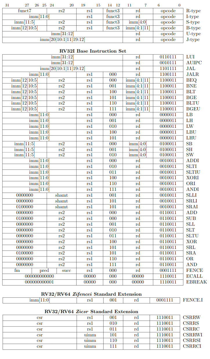
Core RV32I ISA operations
Each operation is described in more detail in the corresponding chapter of the unprivileged specification, mostly the one titled “RV32I Base Instruction Set”. The privileged specification also contains more information about the CSR instructions, and the registers which they interact with.
It can be confusing and error-prone to represent bitfields as raw values in your code. Instead of checking with m.If( value == 0b1100011 ):, it’s nicer to use something like with m.If( value == OP_BRANCH ):. Using names also lets you distinguish the context which values are being used in: in the table above, a funct3 value of 0b010 could represent a CSRRS, LW, SW, or SLT instruction depending on the 7-bit opcode. One easy way to handle this is by putting a long list of definitions in a global file called something like isa.py, which you can include in all of your modules:
################################################
# RISC-V RV32I definitions and helper methods. #
################################################

from nmigen import *

# Instruction field definitions.
# RV32I opcode definitions:
OP_LUI    = 0b0110111
OP_AUIPC  = 0b0010111
OP_JAL    = 0b1101111
OP_JALR   = 0b1100111
OP_BRANCH = 0b1100011
OP_LOAD   = 0b0000011
OP_STORE  = 0b0100011
OP_REG    = 0b0110011
OP_IMM    = 0b0010011
OP_SYSTEM = 0b1110011
OP_FENCE  = 0b0001111
# RV32I "funct3" bits. These select different functions with
# R-type, I-type, S-type, and B-type instructions.
F_JALR    = 0b000
F_BEQ     = 0b000
F_BNE     = 0b001
F_BLT     = 0b100
F_BGE     = 0b101
F_BLTU    = 0b110
F_BGEU    = 0b111
F_LB      = 0b000
F_LH      = 0b001
F_LW      = 0b010
F_LBU     = 0b100
F_LHU     = 0b101
F_SB      = 0b000
F_SH      = 0b001
F_SW      = 0b010
F_ADDI    = 0b000
F_SLTI    = 0b010
F_SLTIU   = 0b011
F_XORI    = 0b100
F_ORI     = 0b110
F_ANDI    = 0b111
F_SLLI    = 0b001
F_SRLI    = 0b101
F_SRAI    = 0b101
F_ADD     = 0b000
F_SUB     = 0b000
F_SLL     = 0b001
F_SLT     = 0b010
F_SLTU    = 0b011
F_XOR     = 0b100
F_SRL     = 0b101
F_SRA     = 0b101
F_OR      = 0b110
F_AND     = 0b111
# RV32I "funct7" bits. Along with the "funct3" bits, these select
# different functions with R-type instructions.
FF_SLLI   = 0b0000000
FF_SRLI   = 0b0000000
FF_SRAI   = 0b0100000
FF_ADD    = 0b0000000
FF_SUB    = 0b0100000
FF_SLL    = 0b0000000
FF_SLT    = 0b0000000
FF_SLTU   = 0b0000000
FF_XOR    = 0b0000000
FF_SRL    = 0b0000000
FF_SRA    = 0b0100000
FF_OR     = 0b0000000
FF_AND    = 0b0000000
# CSR definitions, for 'ECALL' system instructions.
# Like with other "I-type" instructions, the 'funct3' bits select
# between different types of environment calls.
F_TRAPS  = 0b000
F_CSRRW  = 0b001
F_CSRRS  = 0b010
F_CSRRC  = 0b011
F_CSRRWI = 0b101
F_CSRRSI = 0b110
F_CSRRCI = 0b111
# Definitions for non-CSR 'ECALL' system instructions. These seem to
# use the whole 12-bit immediate to encode their functionality.
IMM_MRET = 0x302
IMM_WFI  = 0x105
# ID numbers for different types of traps (exceptions).
TRAP_IMIS  = 1
TRAP_ILLI  = 2
TRAP_BREAK = 3
TRAP_LMIS  = 4
TRAP_SMIS  = 6
TRAP_ECALL = 11
# (etc...)
You can also add a few helper methods for common HDL or simulation operations:
# Flip a word of data.
def FLIP( v ):
  return Cat( v[ 31 - i ] for i in range( 0, 32 ) )

# Convert a 32-bit word to little-endian byte format.
# 0x1234ABCD -> 0xCDAB3412
def LITTLE_END( v ):
  return ( ( ( v & 0x000000FF ) << 24 ) |
           ( ( v & 0x0000FF00 ) << 8  ) |
           ( ( v & 0x00FF0000 ) >> 8  ) |
           ( ( v & 0xFF000000 ) >> 24 ) )
# Little-end conversion for use within an nMigen design.
def LITTLE_END_L( v ):
  # Seems faster, but more LUTs.
  return Cat( v[ 24 : 32 ], v[ 16 : 24 ], v[ 8 : 16 ], v[ 0 : 8 ] )
  # Seems slower, but fewer LUTs.
  #return LITTLE_END( v )

# Helper method to pretty-print a 2s-complement 32-bit hex string.
def hexs( h ):
  if h >= 0:
    return "0x%08X"%( h )
  else:
    return "0x%08X"%( ( h + ( 1 << 32 ) ) % ( 1 << 32 ) )
You might come up with other things to add to this sort of global definitions file, but that should cover most of the basics. You can see what I ended up with on GitHub, although that file includes some things which we won’t talk about until later in this post.
If you’re feeling confused at this point, you might want to skim the “RV32I Base Integer Instruction Set” and “Zicsr Control and Status Register (CSR) Instructions” chapters in the unprivileged specification and the “Machine-Level ISA” chapter in the privileged one. You can ignore anything regarding user, supervisor, and hypervisor modes in the privileged specification. The unprivileged spec’s “Introduction” chapter is also pretty brief and legible, if you feel unsure of what exactly the RISC-V specification aims to specify.
Once you have a basic grasp of the sorts of operations that we will be implementing, let’s move on to implementing the ALU to perform the CPU’s basic math operations.
ALU: the Arithmetic and Logic Unit
An ALU is conceptually simple: it has two inputs, one output, and a ‘function select’ field which determines how the inputs are operated on to produce the output. It’s basically a multiplexer which selects between different arithmetic and logic operations.
With the core RV32I ISA, we can determine which operation should be performed by checking the 3 funct3 bits and the 2nd-most-significant bit of funct7. You can use any arbitrary values to describe the ALU operations, but if you use bits that already exist in the instruction format, you can send those bits directly to a module instead of performing extra hardware logic to translate between values. So here are the 4-bit ‘function select’ definitions that I put in the isa.py file:
# ALU operation definitions. These implement the logic behind math
# instructions, e.g. 'ADD' covers 'ADD', 'ADDI', etc.
ALU_ADD   = 0b0000
ALU_SUB   = 0b1000
ALU_SLT   = 0b0010
ALU_SLTU  = 0b0011
ALU_XOR   = 0b0100
ALU_OR    = 0b0110
ALU_AND   = 0b0111
ALU_SLL   = 0b0001
ALU_SRL   = 0b0101
ALU_SRA   = 0b1101
# String mappings for opcodes, function bits, etc.
ALU_STRS = {
  ALU_ADD:  "+", ALU_SLT:  "<", ALU_SLTU: "<",
  ALU_XOR:  "^", ALU_OR:   "|", ALU_AND:  "&",
  ALU_SLL: "<<", ALU_SRL: ">>", ALU_SRA: ">>",
  ALU_SUB:  "-"
}
You can also use the same ALU operation for different instructions if they perform the same logic. For example, the SLL and SLLI instructions both use the ALU_SLL function select bits. When we implement the actual instructions in the CPU, we’ll change the ALU input fields while using the same ‘function select’ bits. If you look back to the table in the last section, you’ll see that while the opcodes are different, the funct3 bits are identical for ADD / ADDI, SLL / SLLI, etc.
Anyways, a basic ALU module’s initialization only needs to include the four signals mentioned above: inputs (a and b), output (y), and ‘function select’ bits (f):
from nmigen import *
from nmigen.back.pysim import *

from isa import *

import sys

###############
# ALU module: #
###############

class ALU( Elaboratable ):
  def __init__( self ):
    # 'A' and 'B' data inputs.
    self.a = Signal( 32, reset = 0x00000000 )
    self.b = Signal( 32, reset = 0x00000000 )
    # 'F' function select input.
    self.f = Signal( 4,  reset = 0b0000 )
    # 'Y' data output.
    self.y = Signal( 32, reset = 0x00000000 )
Most architectures would also add conditional flags here like n, z, and v to indicate when the last operation was negative, equal to zero, or overflowed. But the RISC-V architecture omits that common feature, so I didn’t include any.
The actual logic of an ALU module can also be pretty simple in nMigen: simply perform a different math operation depending on the f value. I used a switch case, but you could also use a chain of with m.If(...): / with m.Elif(...): statements to synthesize the module as a multiplexer.
And thanks to some advice from the #nmigen channel on freenode, I implemented the left- and right-shift operations using only right shifts. Later, in the CPU module, the inputs and output of left shift operations will be flipped before and after the ALU processes them. That might sound convoluted, but 32-bit shift operations use a lot of hardware, so omitting one of the two 32-bit barrel shifters ends up being worth the extra complexity. Subtraction is implemented as A + (-B) for the same reason, to reduce the number of big and arbitrary 32-bit operations that the synthesizer needs to include in the design.
  def elaborate( self, platform ):
    # Core ALU module.
    m = Module()

    # Dummy synchronous logic only for simulation.
    if platform is None:
      ta = Signal()
      m.d.sync += ta.eq( ~ta )

    # Perform ALU computations based on the 'function' bits.
    with m.Switch( self.f[ :3 ] ):
      # Y = A AND B
      with m.Case( ALU_AND & 0b111 ):
        m.d.comb += self.y.eq( self.a & self.b )
      # Y = A  OR B
      with m.Case( ALU_OR & 0b111 ):
        m.d.comb += self.y.eq( self.a | self.b )
      # Y = A XOR B
      with m.Case( ALU_XOR & 0b111 ):
        m.d.comb += self.y.eq( self.a ^ self.b )
      # Y = A +/- B
      # Subtraction is implemented as A + (-B).
      with m.Case( ALU_ADD & 0b111 ):
        m.d.comb += self.y.eq(
          self.a.as_signed() + Mux( self.f[ 3 ],
            ( ~self.b + 1 ).as_signed(),
            self.b.as_signed() ) )
      # Y = ( A < B ) (signed)
      with m.Case( ALU_SLT & 0b111 ):
        m.d.comb += self.y.eq( self.a.as_signed() < self.b.as_signed() )
      # Y = ( A <  B ) (unsigned)
      with m.Case( ALU_SLTU & 0b111 ):
        m.d.comb += self.y.eq( self.a < self.b )
      # Note: Shift operations cannot shift more than XLEN (32) bits.
      # Also, left shifts are implemented by flipping the inputs
      # and outputs of a right shift operation in the CPU logic.
      # Y = A >> B
      with m.Case( ALU_SRL & 0b111 ):
        m.d.comb += self.y.eq( Mux( self.f[ 3 ],
          self.a.as_signed() >> ( self.b[ :5 ] ),
          self.a >> ( self.b[ :5 ] ) ) )

    # End of ALU module definition.
    return m
Mux( c, a, b ) is an nMigen function which creates a multiplexer, equivalent to a ternary expression in most languages (c ? a : b): if condition c is zero, b gets run. Otherwise, a gets run. It is roughly equivalent to this code, but less verbose:
with m.If( c ):
  a
with m.Else():
  b
And don’t forget that with m.If(...): / with m.Else(): is not the same as the usual Python if ...: / else: syntax. The former condition is synthesized into the design to be evaluated at runtime, while the latter is evaluated once when the design is built. The nMigen Mux(...) function acts like with m.If(...): / with m.Else():, so you can use it to represent simple if / else decisions in your design.
The x[ :5 ] syntax also works like Python’s slice notation to select a range of bits from a signal, in this case to select the 5 least significant bits in signal x. You can also use the x.bit_select(start, N) function to get N bits out of a signal starting at bit start. So self.b[ :5 ] is equivalent to self.b.bit_select( 0, 5 ).
Some operations need to treat the inputs as twos-complement signed values instead of unsigned ones. You can convert between representations in nMigen with .as_signed() and .as_unsigned(), but keep in mind that those operations are not free in terms of resource usage. Signals are unsigned by default, but you can define a 32-bit signed Signal using the shape attribute instead of a numeric width:
Signal( shape = Shape( width = 32, signed = True ) )
Finally, there’s some dummy synchronous logic near the top of the elaborate method which is only included when the design is simulated. It’s there for the testbench, because you’ll get an error if you try to synchronously simulate a module where the sync domain is not used.
Speaking of testing, it’s a good idea to simulate and test as much of each module as you can in an FPGA design. It’s much harder to debug hardware designs than software, and you can catch problems much more quickly in a simulation. It can also be easier to narrow down why your CPU stopped working after a change if you can run some fast tests for individual submodules like the ALU and memories.
Remember that you can append testbench logic after a module definition in the same Python file, so this code can also go in alu.py. First, let’s define a helper method to run an individual ALU unit test. All that it needs to do is set the a, b, and f inputs, wait a tick, then read the y output. And for unit testing, it should also compare the output to the expected result and print a pass / fail message:
##################
# ALU testbench: #
##################
# Keep track of test pass / fail rates.
p = 0
f = 0

# Perform an individual ALU unit test.
def alu_ut( alu, a, b, fn, expected ):
  global p, f
  # Set A, B, F.
  yield alu.a.eq( a )
  yield alu.b.eq( b )
  yield alu.f.eq( fn )
  # Wait a clock tick.
  yield Tick()
  # Done. Check the result after combinatorial logic settles.
  yield Settle()
  actual = yield alu.y
  if hexs( expected ) != hexs( actual ):
    f += 1
    print( "\033[31mFAIL:\033[0m %s %s %s = %s (got: %s)"
           %( hexs( a ), ALU_STRS[ fn ], hexs( b ),
              hexs( expected ), hexs( actual ) ) )
  else:
    p += 1
    print( "\033[32mPASS:\033[0m %s %s %s = %s"
           %( hexs( a ), ALU_STRS[ fn ],
              hexs( b ), hexs( expected ) ) )
This test method uses some of the helpers that we defined in the isa.py file to pretty-print the results. The ALU_STRS dictionary converts the ‘function select’ bits to a string which represents the operation (like +, &, etc.). And hexs(...) prints signed integers in hexadecimal format.
So to test that 4 + 2 = 6, we can run alu_ut( alu, 4, 2, ALU_ADD, 6 ). Here’s the test method that I ended up using. It’s not comprehensive, but we will run the official compliance tests later to test each operation more completely:
# Top-level ALU test method.
def alu_test( alu ):
  # Let signals settle after reset.
  yield Settle()

  # Print a test header.
  print( "--- ALU Tests ---" )

  # Test the bitwise 'AND' operation.
  print( "AND (&) tests:" )
  yield from alu_ut( alu, 0xCCCCCCCC, 0xCCCC0000, ALU_AND, 0xCCCC0000 )
  yield from alu_ut( alu, 0x00000000, 0x00000000, ALU_AND, 0x00000000 )
  yield from alu_ut( alu, 0xFFFFFFFF, 0xFFFFFFFF, ALU_AND, 0xFFFFFFFF )
  yield from alu_ut( alu, 0x00000000, 0xFFFFFFFF, ALU_AND, 0x00000000 )
  yield from alu_ut( alu, 0xFFFFFFFF, 0x00000000, ALU_AND, 0x00000000 )

  # Test the bitwise 'OR' operation.
  print( "OR  (|) tests:" )
  yield from alu_ut( alu, 0xCCCCCCCC, 0xCCCC0000, ALU_OR, 0xCCCCCCCC )
  yield from alu_ut( alu, 0x00000000, 0x00000000, ALU_OR, 0x00000000 )
  yield from alu_ut( alu, 0xFFFFFFFF, 0xFFFFFFFF, ALU_OR, 0xFFFFFFFF )
  yield from alu_ut( alu, 0x00000000, 0xFFFFFFFF, ALU_OR, 0xFFFFFFFF )
  yield from alu_ut( alu, 0xFFFFFFFF, 0x00000000, ALU_OR, 0xFFFFFFFF )

  # Test the bitwise 'XOR' operation.
  print( "XOR (^) tests:" )
  yield from alu_ut( alu, 0xCCCCCCCC, 0xCCCC0000, ALU_XOR, 0x0000CCCC )
  yield from alu_ut( alu, 0x00000000, 0x00000000, ALU_XOR, 0x00000000 )
  yield from alu_ut( alu, 0xFFFFFFFF, 0xFFFFFFFF, ALU_XOR, 0x00000000 )
  yield from alu_ut( alu, 0x00000000, 0xFFFFFFFF, ALU_XOR, 0xFFFFFFFF )
  yield from alu_ut( alu, 0xFFFFFFFF, 0x00000000, ALU_XOR, 0xFFFFFFFF )

  # Test the addition operation.
  print( "ADD (+) tests:" )
  yield from alu_ut( alu, 0, 0, ALU_ADD, 0 )
  yield from alu_ut( alu, 0, 1, ALU_ADD, 1 )
  yield from alu_ut( alu, 1, 0, ALU_ADD, 1 )
  yield from alu_ut( alu, 0xFFFFFFFF, 1, ALU_ADD, 0 )
  yield from alu_ut( alu, 29, 71, ALU_ADD, 100 )
  yield from alu_ut( alu, 0x80000000, 0x80000000, ALU_ADD, 0 )
  yield from alu_ut( alu, 0x7FFFFFFF, 0x7FFFFFFF, ALU_ADD, 0xFFFFFFFE )

  # Test the subtraction operation.
  print( "SUB (-) tests:" )
  yield from alu_ut( alu, 0, 0, ALU_SUB, 0 )
  yield from alu_ut( alu, 0, 1, ALU_SUB, -1 )
  yield from alu_ut( alu, 1, 0, ALU_SUB, 1 )
  yield from alu_ut( alu, -1, 1, ALU_SUB, -2 )
  yield from alu_ut( alu, 1, -1, ALU_SUB, 2 )
  yield from alu_ut( alu, 29, 71, ALU_SUB, -42 )
  yield from alu_ut( alu, 0x80000000, 1, ALU_SUB, 0x7FFFFFFF )
  yield from alu_ut( alu, 0x7FFFFFFF, -1, ALU_SUB, 0x80000000 )

  # Test the signed '<' comparison operation.
  print( "SLT (signed <) tests:" )
  yield from alu_ut( alu, 0, 0, ALU_SLT, 0 )
  yield from alu_ut( alu, 1, 0, ALU_SLT, 0 )
  yield from alu_ut( alu, 0, 1, ALU_SLT, 1 )
  yield from alu_ut( alu, -1, 0, ALU_SLT, 1 )
  yield from alu_ut( alu, -42, -10, ALU_SLT, 1 )
  yield from alu_ut( alu, -10, -42, ALU_SLT, 0 )

  # Test the unsigned '<' comparison operation.
  print( "SLTU (unsigned <) tests:" )
  yield from alu_ut( alu, 0, 0, ALU_SLTU, 0 )
  yield from alu_ut( alu, 1, 0, ALU_SLTU, 0 )
  yield from alu_ut( alu, 0, 1, ALU_SLTU, 1 )
  yield from alu_ut( alu, -1, 0, ALU_SLTU, 0 )
  yield from alu_ut( alu, -42, -10, ALU_SLTU, 1 )
  yield from alu_ut( alu, -10, -42, ALU_SLTU, 0 )
  yield from alu_ut( alu, -42, 42, ALU_SLTU, 0 )

  # Test the shift right operation.
  print ( "SRL (>>) tests:" )
  yield from alu_ut( alu, 0x00000001, 0, ALU_SRL, 0x00000001 )
  yield from alu_ut( alu, 0x00000001, 1, ALU_SRL, 0x00000000 )
  yield from alu_ut( alu, 0x00000011, 1, ALU_SRL, 0x00000008 )
  yield from alu_ut( alu, 0x00000010, 1, ALU_SRL, 0x00000008 )
  yield from alu_ut( alu, 0x80000000, 1, ALU_SRL, 0x40000000 )
  yield from alu_ut( alu, 0x80000000, 4, ALU_SRL, 0x08000000 )

  # Test the shift right with sign extension operation.
  print ( "SRA (>> + sign extend) tests:" )
  yield from alu_ut( alu, 0x00000001, 0, ALU_SRA, 0x00000001 )
  yield from alu_ut( alu, 0x00000001, 1, ALU_SRA, 0x00000000 )
  yield from alu_ut( alu, 0x00000011, 1, ALU_SRA, 0x00000008 )
  yield from alu_ut( alu, 0x00000010, 1, ALU_SRA, 0x00000008 )
  yield from alu_ut( alu, 0x80000000, 1, ALU_SRA, 0xC0000000 )
  yield from alu_ut( alu, 0x80000000, 4, ALU_SRA, 0xF8000000 )

  # Done.
  yield Tick()
  print( "ALU Tests: %d Passed, %d Failed"%( p, f ) )
I didn’t include the SLL left-shift operation, since the logic to flip those inputs and outputs will be handled outside of the ALU, but you could add a few tests using the FLIP method from our isa.py file if you want:
alu_ut( alu, FLIP( a ), b, ALU_SLL, FLIP( expected_output ) )
Finally, you’ll need some logic to run the testbench when the alu.py file is run. This looks very similar to the testbench logic from my last nMigen post, because the library makes it very easy to run a simple simulation:
# 'main' method to run a basic testbench.
if __name__ == "__main__":
  # Instantiate an ALU module.
  dut = ALU()

  # Run the tests.
  with Simulator( dut, vcd_file = open( 'alu.vcd', 'w' ) ) as sim:
    def proc():
      yield from alu_test( dut )
    sim.add_clock( 1e-6 )
    sim.add_sync_process( proc )
    sim.run()
Now, even though we haven’t written any CPU logic yet, you should be able to run python3 alu.py and see that the unit tests pass:
--- ALU Tests ---
AND (&) tests:
PASS: 0xCCCCCCCC & 0xCCCC0000 = 0xCCCC0000
PASS: 0x00000000 & 0x00000000 = 0x00000000
PASS: 0xFFFFFFFF & 0xFFFFFFFF = 0xFFFFFFFF
PASS: 0x00000000 & 0xFFFFFFFF = 0x00000000
PASS: 0xFFFFFFFF & 0x00000000 = 0x00000000
OR  (|) tests:
PASS: 0xCCCCCCCC | 0xCCCC0000 = 0xCCCCCCCC
PASS: 0x00000000 | 0x00000000 = 0x00000000
[...more tests...]
SRA (>> + sign extend) tests:
PASS: 0x00000001 >> 0x00000000 = 0x00000001
PASS: 0x00000001 >> 0x00000001 = 0x00000000
PASS: 0x00000011 >> 0x00000001 = 0x00000008
PASS: 0x00000010 >> 0x00000001 = 0x00000008
PASS: 0x80000000 >> 0x00000001 = 0xC0000000
PASS: 0x80000000 >> 0x00000004 = 0xF8000000
ALU Tests: 55 Passed, 0 Failed
The PASS messages should be green, and FAILs should turn up red. That’s what the funny-looking string fragments like \033[31m in the print statements are for: they’re terminal color codes, although not every type of shell will support them. And while it is really tempting to use the \033[5m option to put blinking text in your terminal outputs, trust me: your colleagues probably won’t think it’s as funny as you do 🙂
Anyways, that should give us a working ALU; you can find a full alu.py file on GitHub. Next, we need some working memory modules.
RAM, ROM, and Memory Spaces
Most microcontrollers come with two kinds of memory: fast volatile RAM, and slow non-volatile Flash. But there are exceptions, like the MSP430s which use non-volatile FRAM, or Espressif’s popular ESP8266 and ESP32 chips which don’t include general-purpose non-volatile memory. iCE40 FPGAs also lack built-in Flash memory, but like the Espressif chips, boards which use them almost always include an external SPI Flash chip to serve that function.
I talked about how to use a connected SPI Flash chip as read-only ‘program memory’ through a Wishbone bus in my last nMigen post. I took a similar approach with this CPU design to make a rom.py module for quickly simulating test programs, and a spi_rom.py module for reading program data off of an actual Flash chip. And since the SPI Flash chip is treated as read-only, there’s also a slightly more complex ram.py module which uses the FPGA’s RAM resources as volatile read / write memory.
All of the memory modules use the same Wishbone bus interface, so the CPU logic which accesses them can use the same bus signals regardless of what type of memory is being addressed. They’ll also use Arbiter objects to provide multiple bus Interfaces which can each be used by different parts of our design, and Decoder objects to choose which module to access based on the memory address space. Later on, we’ll add peripherals which implement the same Wishbone bus Interface class, and those will also be added to the Decoders to allow the CPU to access peripheral registers with load / store instructions.
The nmigen-soc library includes a Wishbone bus Interface implementation as well as the Decoder and Arbiter helper classes, so this all ends up being simpler to implement than you might think.
Simulated ROM
The simulated ROM module is simplest, so let’s start with that. It’s very similar to the one in my last post, but it uses a bus arbiter and is byte-addressed instead of word-addressed. The initialization code is straightforward:
from nmigen import *
from math import ceil, log2
from nmigen.back.pysim import *
from nmigen_soc.memory import *
from nmigen_soc.wishbone import *

from isa import *

###############
# ROM module: #
###############

class ROM( Elaboratable ):
  def __init__( self, data ):
    # Data storage.
    self.data = Memory( width = 32, depth = len( data ), init = data )
    # Memory read port.
    self.r = self.data.read_port()
    # Record size.
    self.size = len( data ) * 4
    # Initialize Wishbone bus arbiter.
    self.arb = Arbiter( addr_width = ceil( log2( self.size + 1 ) ),
                        data_width = 32 )
    self.arb.bus.memory_map = MemoryMap(
      addr_width = self.arb.bus.addr_width,
      data_width = self.arb.bus.data_width,
      alignment = 0 )
Like with the Interface objects in my last nMigen post, the Arbiter‘s MemoryMap attribute needs to be defined to prevent build errors, but it can be set up as an empty object when you don’t have any particular mapping in mind.
And since we’re using a bus arbiter to mediate bus access from different parts of the design, I also include a new_bus method which creates a new Wishbone bus Interface, adds it to the Arbiter, and then returns the new Interface:
  def new_bus( self ):
    # Initialize a new Wishbone bus interface.
    bus = Interface( addr_width = self.arb.bus.addr_width,
                     data_width = self.arb.bus.data_width )
    bus.memory_map = MemoryMap( addr_width = bus.addr_width,
                                data_width = bus.data_width,
                                alignment = 0 )
    self.arb.add( bus )
    return bus
This might seem like an odd pattern, but it will give us the option of letting peripherals access memory directly later on. One example of a peripheral which might require memory access is DMA, which moves data without intervention from the CPU. Or you might want to let a peripheral stream data into or out of a buffer on its own; for example, I’ve written a “neopixel” peripheral which can send color data to addressable LEDs directly from a RAM buffer, but this post is getting too long to review that in detail.
Anyways, since ROM is read-only, the runtime logic for the rom.py module is pretty simple:
  def elaborate( self, platform ):
    m = Module()
    m.submodules.arb = self.arb
    m.submodules.r = self.r

    # Ack two cycles after activation, for memory port access and
    # synchronous read-out (to prevent combinatorial loops).
    rws = Signal( 1, reset = 0 )
    m.d.sync += [
      rws.eq( self.arb.bus.cyc ),
      self.arb.bus.ack.eq( self.arb.bus.cyc & rws )
    ]

    # Set read port address (in words).
    m.d.comb += self.r.addr.eq( self.arb.bus.adr >> 2 )

    # Set the 'output' value to the requested 'data' array index.
    # If a read would 'spill over' into an out-of-bounds data byte,
    # set that byte to 0x00.
    # Word-aligned reads
    with m.If( ( self.arb.bus.adr & 0b11 ) == 0b00 ):
      m.d.sync += self.arb.bus.dat_r.eq( LITTLE_END_L( self.r.data ) )
    # Un-aligned reads
    with m.Else():
      m.d.sync += self.arb.bus.dat_r.eq(
        LITTLE_END_L( self.r.data << ( ( self.arb.bus.adr & 0b11 ) << 3 ) ) )

    # End of ROM module definition.
    return m
We don’t need to have this module read across word boundaries, because the RISC-V specification lets us raise an exception for mis-aligned memory access. That logic will go in the CPU module later on. You could allow these memory modules to perform cross-word reads and writes, but the logic would be more complex and I think it would result in a larger design. You’d either need to perform memory access across multiple cycles, or attach multiple read/write ports to the backing Memory object.
Notice that the output values are converted to little-endian format using the LITTLE_END_L helper method from isa.py. The specification allows a CPU to be either big- or little-endian, but it strongly encourages little-endianness, and that is how GCC will compile our code by default.
Moving on to the testbench, I used the same structure as the ALU tests. First, there’s a “unit test” method which tests an individual read cycle:
##################
# ROM testbench: #
##################
# Keep track of test pass / fail rates.
p = 0
f = 0

# Perform an individual ROM unit test.
def rom_read_ut( rom, address, expected ):
  global p, f
  # Set address, and wait two ticks.
  yield rom.arb.bus.adr.eq( address )
  yield Tick()
  yield Tick()
  # Done. Check the result after combinational logic settles.
  yield Settle()
  actual = yield rom.arb.bus.dat_r
  if expected != actual:
    f += 1
    print( "\033[31mFAIL:\033[0m ROM[ 0x%08X ] = 0x%08X (got: 0x%08X)"
           %( address, expected, actual ) )
  else:
    p += 1
    print( "\033[32mPASS:\033[0m ROM[ 0x%08X ] = 0x%08X"
           %( address, expected ) )
Next, there’s a test method which defines a series of unit tests to simulate running:
# Top-level ROM test method.
def rom_test( rom ):
  global p, f

  # Let signals settle after reset.
  yield Settle()

  # Print a test header.
  print( "--- ROM Tests ---" )

  # Assert 'cyc' to activate the bus.
  yield rom.arb.bus.cyc.eq( 1 )
  # Test the ROM's "happy path" (reading valid data).
  yield from rom_read_ut( rom, 0x0, LITTLE_END( 0x01234567 ) )
  yield from rom_read_ut( rom, 0x4, LITTLE_END( 0x89ABCDEF ) )
  yield from rom_read_ut( rom, 0x8, LITTLE_END( 0x42424242 ) )
  yield from rom_read_ut( rom, 0xC, LITTLE_END( 0xDEADBEEF ) )
  # Test byte-aligned and halfword-aligned addresses.
  yield from rom_read_ut( rom, 0x1, LITTLE_END( 0x23456700 ) )
  yield from rom_read_ut( rom, 0x2, LITTLE_END( 0x45670000 ) )
  yield from rom_read_ut( rom, 0x3, LITTLE_END( 0x67000000 ) )
  yield from rom_read_ut( rom, 0x5, LITTLE_END( 0xABCDEF00 ) )
  yield from rom_read_ut( rom, 0x6, LITTLE_END( 0xCDEF0000 ) )
  yield from rom_read_ut( rom, 0x7, LITTLE_END( 0xEF000000 ) )
  # Test reading the last few bytes of data.
  yield from rom_read_ut( rom, rom.size - 4, LITTLE_END( 0xDEADBEEF ) )
  yield from rom_read_ut( rom, rom.size - 3, LITTLE_END( 0xADBEEF00 ) )
  yield from rom_read_ut( rom, rom.size - 2, LITTLE_END( 0xBEEF0000 ) )
  yield from rom_read_ut( rom, rom.size - 1, LITTLE_END( 0xEF000000 ) )

  # Done.
  yield Tick()
  print( "ROM Tests: %d Passed, %d Failed"%( p, f ) )
Finally, there’s the Python __main__ method which simulates the tests when the rom.py file is run:
# 'main' method to run a basic testbench.
if __name__ == "__main__":
  # Instantiate a test ROM module with 16 bytes of data.
  dut = ROM( [ 0x01234567, 0x89ABCDEF, 0x42424242, 0xDEADBEEF ] )

  # Run the ROM tests.
  with Simulator( dut, vcd_file = open( 'rom.vcd', 'w' ) ) as sim:
    def proc():
      yield from rom_test( dut )
    sim.add_clock( 1e-6 )
    sim.add_sync_process( proc )
    sim.run()
You should be able to run python3 rom.py and see that the unit tests pass. Sadly though, we can’t actually use this module to store non-volatile program data, because Memory objects use volatile “block RAM” hardware in the chip. There isn’t very much of that kind of RAM available, so next, let’s write a module to use the external SPI Flash as non-volatile program storage.
And like the rest of these modules, you can find a full rom.py file on GitHub.
SPI Flash ‘ROM’
Again, this module will look similar to the spi_rom.py module from my last nMigen post. First, I added DummyPin and DummySPI classes to use during simulations. I think that it may be possible to use one of nMigen’s built-in classes for this sort of thing, like Pin. But I haven’t quite figured out how, so:
from nmigen import *
from math import ceil, log2
from nmigen.back.pysim import *
from nmigen_soc.memory import *
from nmigen_soc.wishbone import *
from nmigen_boards.resources import *

from isa import *

###########################
# SPI Flash "ROM" module: #
###########################

# (Dummy SPI resources for simulated tests)
class DummyPin():
  def __init__( self, name ):
    self.o = Signal( name = '%s_o'%name )
    self.i = Signal( name = '%s_i'%name )
class DummySPI():
  def __init__( self ):
    self.cs   = DummyPin( 'cs' )
    self.clk  = DummyPin( 'clk' )
    self.mosi = DummyPin( 'mosi' )
    self.miso = DummyPin( 'miso' )
The SPI_ROM class initialization contains some signals to support the SPI communication, a bus arbiter, and a backing Memory store for when the module is being simulated instead of running on real hardware:
# Core SPI Flash "ROM" module.
class SPI_ROM( Elaboratable ):
  def __init__( self, dat_start, dat_end, data ):
    # Starting address in the Flash chip. This probably won't
    # be zero, because many FPGA boards use their external SPI
    # Flash to store the bitstream which configures the chip.
    self.dstart = dat_start
    # Last accessible address in the flash chip.
    self.dend = dat_end
    # Length of accessible data.
    self.dlen = ( dat_end - dat_start ) + 1
    # SPI Flash address command.
    self.spio = Signal( 32, reset = 0x03000000 )
    # Data counter.
    self.dc = Signal( 6, reset = 0b000000 )

    # Backing data store for a test ROM image. Not used when
    # the module is built for real hardware.
    if data is not None:
      self.data = Memory( width = 32, depth = len( data ), init = data )
    else:
      self.data = None

    # Initialize Wishbone bus arbiter.
    self.arb = Arbiter( addr_width = ceil( log2( self.dlen + 1 ) ),
                        data_width = 32 )
    self.arb.bus.memory_map = MemoryMap(
      addr_width = self.arb.bus.addr_width,
      data_width = self.arb.bus.data_width,
      alignment = 0 )
There’s also the same new_bus method that the ROM module had, to create a new Wishbone bus Interface and add it to the module’s bus Arbiter:
  def new_bus( self ):
    # Initialize a new Wishbone bus interface.
    bus = Interface( addr_width = self.arb.bus.addr_width,
                     data_width = self.arb.bus.data_width )
    bus.memory_map = MemoryMap( addr_width = bus.addr_width,
                                data_width = bus.data_width,
                                alignment = 0 )
    self.arb.add( bus )
    return bus
And finally, there’s the same SPI read logic as I used in my last nMigen post. You can read that post for more information, but it is basically a state machine with “power-on”, “waiting”, “transmit”, and “receive” states. When the device first powers on, it sends a “wake up” command to the SPI Flash chip, because iCE40 FPGAs put their Flash modules to sleep after loading their configuration bitstreams. After that, the mdoule waits for a read request on the Wishbone bus, transmits a “read data” command with the desired 24-bit address over SPI, and receives a word of data in little-endian format. There is no caching, which will make the CPU quite slow when it executes code from Flash. But this works as a minimal implementation:
  def elaborate( self, platform ):
    m = Module()
    m.submodules.arb = self.arb

    if platform is None:
      self.spi = DummySPI()
    else:
      self.spi = platform.request( 'spi_flash_1x' )

    # Clock rests at 0.
    m.d.comb += self.spi.clk.o.eq( 0 )

    # Use a state machine for Flash access.
    # "Mode 0" SPI is very simple:
    # - Device is active when CS is low, inactive otherwise.
    # - Clock goes low, both sides write their bit if necessary.
    # - Clock goes high, both sides read their bit if necessary.
    # - Repeat ad nauseum.
    with m.FSM() as fsm:
      # 'Reset' and 'power-up' states:
      # pull CS low, then release power-down mode by sending 0xAB.
      # Normally this is not necessary, but iCE40 chips shut down
      # their connected SPI Flash after configuring themselves
      # in order to save power and prevent unintended writes.
      with m.State( "SPI_RESET" ):
        m.d.sync += [
          self.spi.cs.o.eq( 1 ),
          self.spio.eq( 0xAB000000 )
        ]
        m.next = "SPI_POWERUP"
      with m.State( "SPI_POWERUP" ):
        m.d.comb += [
          self.spi.clk.o.eq( ~ClockSignal( "sync" ) ),
          self.spi.mosi.o.eq( self.spio[ 31 ] )
        ]
        m.d.sync += [
          self.spio.eq( self.spio << 1 ),
          self.dc.eq( self.dc + 1 )
        ]
        m.next = "SPI_POWERUP"
        # Wait a few extra cycles after ending the transaction to
        # allow the chip to wake up from sleep mode.
        # TODO: Time this based on clock frequency?
        with m.If( self.dc == 30 ):
          m.next = "SPI_WAITING"
        # De-assert CS after sending 8 bits of data = 16 clock edges.
        with m.Elif( self.dc >= 8 ):
          m.d.sync += self.spi.cs.o.eq( 0 )
      # 'Waiting' state: Keep the 'cs' pin high until a new read is
      # requested, then move to 'SPI_TX' to send the read command.
      # Also keep 'ack' asserted until 'stb' is released.
      with m.State( "SPI_WAITING" ):
        m.d.sync += [
          self.arb.bus.ack.eq( self.arb.bus.cyc &
            ( self.arb.bus.ack & self.arb.bus.stb ) ),
          self.spi.cs.o.eq( 0 )
        ]
        m.next = "SPI_WAITING"
        with m.If( ( self.arb.bus.cyc == 1 ) &
                   ( self.arb.bus.stb == 1 ) &
                   ( self.arb.bus.ack == 0 ) ):
          m.d.sync += [
            self.spi.cs.o.eq( 1 ),
            self.spio.eq( ( 0x03000000 | ( ( self.arb.bus.adr + self.dstart ) & 0x00FFFFFF ) ) ),
            self.arb.bus.ack.eq( 0 ),
            self.dc.eq( 31 )
          ]
          m.next = "SPI_TX"
      # 'Send read command' state: transmits the 0x03 'read' command
      # followed by the desired 24-bit address. (Encoded in 'spio')
      with m.State( "SPI_TX" ):
        # Set the 'mosi' pin to the next value and increment 'dc'.
        m.d.sync += [
          self.dc.eq( self.dc - 1 ),
          self.spio.eq( self.spio << 1 )
        ]
        m.d.comb += [
          self.spi.clk.o.eq( ~ClockSignal( "sync" ) ),
          self.spi.mosi.o.eq( self.spio[ 31 ] )
        ]
        # Move to 'receive data' state once 32 bits have elapsed.
        # Also clear 'dat_r' and 'dc' before doing so.
        with m.If( self.dc == 0 ):
          m.d.sync += [
            self.dc.eq( 7 ),
            self.arb.bus.dat_r.eq( 0 )
          ]
          m.next = "SPI_RX"
        with m.Else():
          m.next = "SPI_TX"
      # 'Receive data' state: continue the clock signal and read
      # the 'miso' pin on rising edges.
      # You can keep the clock signal going to receive as many bytes
      # as you want, but this implementation only fetches one word.
      with m.State( "SPI_RX" ):
        # Simulate the 'miso' pin value for tests.
        if platform is None:
          with m.If( self.dc < 8 ):
            m.d.comb += self.spi.miso.i.eq( ( self.data[ self.arb.bus.adr >> 2 ] >> ( self.dc + 24 ) ) & 0b1 )
          with m.Elif( self.dc < 16 ):
            m.d.comb += self.spi.miso.i.eq( ( self.data[ self.arb.bus.adr >> 2 ] >> ( self.dc + 8 ) ) & 0b1 )
          with m.Elif( self.dc < 24 ):
            m.d.comb += self.spi.miso.i.eq( ( self.data[ self.arb.bus.adr >> 2 ] >> ( self.dc - 8 ) ) & 0b1 )
          with m.Else():
            m.d.comb += self.spi.miso.i.eq( ( self.data[ self.arb.bus.adr >> 2 ] >> ( self.dc - 24 ) ) & 0b1 )
        m.d.sync += [
          self.dc.eq( self.dc - 1 ),
          self.arb.bus.dat_r.bit_select( self.dc, 1 ).eq( self.spi.miso.i )
        ]
        m.d.comb += self.spi.clk.o.eq( ~ClockSignal( "sync" ) )
        # Assert 'ack' signal and move back to 'waiting' state
        # once a whole word of data has been received.
        with m.If( self.dc[ :3 ] == 0 ):
          with m.If( self.dc[ 3 : 5 ] == 0b11 ):
            m.d.sync += [
              self.spi.cs.o.eq( 0 ),
              self.arb.bus.ack.eq( self.arb.bus.cyc )
            ]
            m.next = "SPI_WAITING"
          with m.Else():
            m.d.sync += self.dc.eq( self.dc + 15 )
            m.next = "SPI_RX"
        with m.Else():
          m.next = "SPI_RX"

    # (End of SPI Flash "ROM" module logic)
    return m
For the testbench, I wanted to test various conditions while simulating the process of reading a word of data out of a SPI Flash module. You can see above that there is special logic to simulate a memory value on the ‘dummy’ MISO pin when the design is being simulated, and I also wanted to verify that the CS signal gets set correctly. So the lowest-level ‘unit tests’ method just compares an ‘expected’ and ‘actual’ value before printing the result:
##############################
# SPI Flash "ROM" testbench: #
##############################
# Keep track of test pass / fail rates.
p = 0
f = 0

# Helper method to record unit test pass/fails.
def spi_rom_ut( name, actual, expected ):
  global p, f
  if expected != actual:
    f += 1
    print( "\033[31mFAIL:\033[0m %s (0x%08X != 0x%08X)"
           %( name, actual, expected ) )
  else:
    p += 1
    print( "\033[32mPASS:\033[0m %s (0x%08X == 0x%08X)"
           %( name, actual, expected ) )
Then there’s a spi_read_word helper method which simulates the process of sending a ‘read data’ command and reading the result. It runs the spi_rom_ut helper after each bit to verify the process:
# Helper method to test reading a byte of SPI data.
def spi_read_word( srom, virt_addr, phys_addr, simword, end_wait ):
  # Set 'address'.
  yield srom.arb.bus.adr.eq( virt_addr )
  # Set 'strobe' and 'cycle' to request a new read.
  yield srom.arb.bus.stb.eq( 1 )
  yield srom.arb.bus.cyc.eq( 1 )
  # Wait a tick; the (inverted) CS pin should then be low, and
  # the 'read command' value should be set correctly.
  yield Tick()
  yield Settle()
  csa = yield srom.spi.cs.o
  spcmd = yield srom.spio
  spi_rom_ut( "CS Low", csa, 1 )
  spi_rom_ut( "SPI Read Cmd Value", spcmd, ( phys_addr & 0x00FFFFFF ) | 0x03000000 )
  # Then the 32-bit read command is sent; two ticks per bit.
  for i in range( 32 ):
    yield Settle()
    dout = yield srom.spi.mosi.o
    spi_rom_ut( "SPI Read Cmd  [%d]"%i, dout, ( spcmd >> ( 31 - i ) ) & 0b1 )
    yield Tick()
  # The following 32 bits should return the word. Simulate
  # the requested word arriving on the MISO pin, MSbit first.
  # (Data starts getting returned on the falling clock edge
  #  immediately following the last rising-edge read.)
  i = 7
  expect = 0
  while i < 32:
    yield Tick()
    yield Settle()
    expect = expect | ( ( 1 << i ) & simword )
    progress = yield srom.arb.bus.dat_r
    spi_rom_ut( "SPI Read Word [%d]"%i, progress, expect )
    if ( ( i & 0b111 ) == 0 ):
      i = i + 15
    else:
      i = i - 1
  # Wait one more tick, then the CS signal should be de-asserted.
  yield Tick()
  yield Settle()
  csa = yield srom.spi.cs.o
  spi_rom_ut( "CS High (Waiting)", csa, 0 )
  # Done; reset 'strobe' and 'cycle' after N ticks to test
  # delayed reads from the bus.
  for i in range( end_wait ):
    yield Tick()
  yield srom.arb.bus.stb.eq( 0 )
  yield srom.arb.bus.cyc.eq( 0 )
  yield Tick()
  yield Settle()
Remember from my last post that the CS signal is inverted in nMigen’s SPI signal representation, so a value of 1 pulls the pin low to activate the connected device. Next, as in the simulated ROM module, the top-level test method simulates reading values out of a few different addresses:
# Top-level SPI ROM test method.
def spi_rom_tests( srom ):
  global p, f

  # Let signals settle after reset.
  yield Tick()
  yield Settle()

  # Print a test header.
  print( "--- SPI Flash 'ROM' Tests ---" )

  # Test basic behavior by reading a few consecutive words.
  yield from spi_read_word( srom, 0x00, 0x200000, LITTLE_END( 0x89ABCDEF ), 0 )
  yield from spi_read_word( srom, 0x04, 0x200004, LITTLE_END( 0x0C0FFEE0 ), 4 )
  # Make sure the CS pin stays de-asserted while waiting.
  for i in range( 4 ):
    yield Tick()
    yield Settle()
    csa = yield srom.spi.cs.o
    spi_rom_ut( "CS High (Waiting)", csa, 0 )
  yield from spi_read_word( srom, 0x10, 0x200010, LITTLE_END( 0xDEADFACE ), 1 )
  yield from spi_read_word( srom, 0x0C, 0x20000C, LITTLE_END( 0xABACADAB ), 1 )

  # Done. Print the number of passed and failed unit tests.
  yield Tick()
  print( "SPI 'ROM' Tests: %d Passed, %d Failed"%( p, f ) )
Finally, the Python __main__ method initializes a SPI_ROM object with simulated program data at a 2MB offset. Remember, the FPGA stores its configuration bitstream starting at address zero, so when we write program data to the Flash chip, its address needs to be offset by a bit:
# 'main' method to run a basic testbench.
if __name__ == "__main__":
  # Instantiate a test SPI ROM module.
  off = ( 2 * 1024 * 1024 )
  dut = SPI_ROM( off, off + 1024, [ 0x89ABCDEF, 0x0C0FFEE0, 0xBABABABA, 0xABACADAB, 0xDEADFACE, 0x12345678, 0x87654321, 0xDEADBEEF, 0xDEADBEEF ] )

  # Run the SPI ROM tests.
  with Simulator( dut, vcd_file = open( 'spi_rom.vcd', 'w' ) ) as sim:
    def proc():
      # Wait until the 'release power-down' command is sent.
      # TODO: test that startup condition.
      for i in range( 30 ):
        yield Tick()
      yield from spi_rom_tests( dut )
    sim.add_clock( 1e-6 )
    sim.add_sync_process( proc )
    sim.run()
And when you run that spi_rom.py file, you should see that the unit tests check the transmitted and received values as they get simulated, bit by bit:
--- SPI Flash 'ROM' Tests ---
PASS: CS Low (0x00000001 == 0x00000001)
PASS: SPI Read Cmd Value (0x03200000 == 0x03200000)
PASS: SPI Read Cmd  [0] (0x00000000 == 0x00000000)
PASS: SPI Read Cmd  [1] (0x00000000 == 0x00000000)
[...more tests...]
PASS: SPI Read Word [26] (0xA8ADACAB == 0xA8ADACAB)
PASS: SPI Read Word [25] (0xAAADACAB == 0xAAADACAB)
PASS: SPI Read Word [24] (0xABADACAB == 0xABADACAB)
PASS: CS High (Waiting) (0x00000000 == 0x00000000)
SPI 'ROM' Tests: 272 Passed, 0 Failed
If you don’t want to copy / paste or type out all of those code blocks, check the example spi_rom.py file.
RAM
Now that we have simulated and in-hardware modules for program data storage, it’s time to write a RAM module which uses the FPGA’s internal RAM for fast read/write memory. This will look similar to the simulated ROM module, with some extra logic to allow writes as well as reads. The initialization logic and new_bus function look almost identical:
from nmigen import *
from math import ceil, log2
from nmigen.back.pysim import *
from nmigen_soc.memory import *
from nmigen_soc.wishbone import *

from isa import *

###############
# RAM module: #
###############

# Data input width definitions.
RAM_DW_8  = 0
RAM_DW_16 = 1
RAM_DW_32 = 2

class RAM( Elaboratable ):
  def __init__( self, size_words ):
    # Record size.
    self.size = ( size_words * 4 )
    # Width of data input.
    self.dw   = Signal( 3, reset = 0b000 )
    # Data storage.
    self.data = Memory( width = 32, depth = size_words,
      init = ( 0x000000 for i in range( size_words ) ) )
    # Read and write ports.
    self.r = self.data.read_port()
    self.w = self.data.write_port()
    # Initialize Wishbone bus arbiter.
    self.arb = Arbiter( addr_width = ceil( log2( self.size + 1 ) ),
                        data_width = 32 )
    self.arb.bus.memory_map = MemoryMap(
      addr_width = self.arb.bus.addr_width,
      data_width = self.arb.bus.data_width,
      alignment = 0 )

  def new_bus( self ):
    # Initialize a new Wishbone bus interface.
    bus = Interface( addr_width = self.arb.bus.addr_width,
                     data_width = self.arb.bus.data_width )
    bus.memory_map = MemoryMap( addr_width = bus.addr_width,
                                data_width = bus.data_width,
                                alignment = 0 )
    self.arb.add( bus )
    return bus
But the class includes a write port as well as a read port, and an extra dw (‘data width’) signal which tells the module how many bytes it should write in the requested word. The RISC-V specification includes load / store instructions for one, two, and four bytes.
The read / write logic is a bit more complex. Access takes three clock cycles in total: first, the address is written to the read and write ports. Then, once data is loaded into the read port, the write port’s data field is set to the new value, which depends on the requested data width. Finally, the write takes a cycle to be applied. As with the simulated ROM module, an rws (‘read wait state’) signal is used to prevent the Wishbone bus’ ack (‘acknowledge’) signal from being asserted too early:
  def elaborate( self, platform ):
    # Core RAM module.
    m = Module()
    m.submodules.r = self.r
    m.submodules.w = self.w
    m.submodules.arb = self.arb

    # Ack two cycles after activation, for memory port access and
    # synchronous read-out (to prevent combinatorial loops).
    rws = Signal( 1, reset = 0 )
    m.d.sync += rws.eq( self.arb.bus.cyc )
    m.d.sync += self.arb.bus.ack.eq( self.arb.bus.cyc & rws )

    m.d.comb += [
      # Set the RAM port addresses.
      self.r.addr.eq( self.arb.bus.adr[ 2: ] ),
      self.w.addr.eq( self.arb.bus.adr[ 2: ] ),
      # Set the 'write enable' flag once the reads are valid.
      self.w.en.eq( self.arb.bus.we )
    ]

    # Read / Write logic: synchronous to avoid combinatorial loops.
    m.d.comb += self.w.data.eq( self.r.data )
    with m.Switch( self.arb.bus.adr[ :2 ] ):
      with m.Case( 0b00 ):
        m.d.sync += self.arb.bus.dat_r.eq( self.r.data )
        with m.Switch( self.dw ):
          with m.Case( RAM_DW_8 ):
            m.d.comb += self.w.data.bit_select( 0, 8 ).eq(
              self.arb.bus.dat_w[ :8 ] )
          with m.Case( RAM_DW_16 ):
            m.d.comb += self.w.data.bit_select( 0, 16 ).eq(
              self.arb.bus.dat_w[ :16 ] )
          with m.Case():
            m.d.comb += self.w.data.eq( self.arb.bus.dat_w )
      with m.Case( 0b01 ):
        m.d.sync += self.arb.bus.dat_r.eq( self.r.data[ 8 : 32 ] )
        with m.Switch( self.dw ):
          with m.Case( RAM_DW_8 ):
            m.d.comb += self.w.data.bit_select( 8, 8 ).eq(
              self.arb.bus.dat_w[ :8 ] )
          with m.Case( RAM_DW_16 ):
            m.d.comb += self.w.data.bit_select( 8, 16 ).eq(
              self.arb.bus.dat_w[ :16 ] )
      with m.Case( 0b10 ):
        m.d.sync += self.arb.bus.dat_r.eq( self.r.data[ 16 : 32 ] )
        with m.Switch( self.dw ):
          with m.Case( RAM_DW_8 ):
            m.d.comb += self.w.data.bit_select( 16, 8 ).eq(
              self.arb.bus.dat_w[ :8 ] )
          with m.Case( RAM_DW_16 ):
            m.d.comb += self.w.data.bit_select( 16, 16 ).eq(
              self.arb.bus.dat_w[ :16 ] )
      with m.Case( 0b11 ):
        m.d.sync += self.arb.bus.dat_r.eq( self.r.data[ 24 : 32 ] )
        with m.Switch( self.dw ):
          with m.Case( RAM_DW_8 ):
            m.d.comb += self.w.data.bit_select( 24, 8 ).eq(
              self.arb.bus.dat_w[ :8 ] )

    # End of RAM module definition.
    return m
I’ve tried a few different ways of handling the read/write logic, and these nested switch cases seemed to yield reasonable performance and size while remaining legible, but I would certainly appreciate suggestions. In a nutshell, the module performs different logic depending on the memory address’ offset relative to a word: 0, 1, 2, or 3 bytes. Since the CPU will raise a memory alignment exception if a read or write would cross a word boundary, we can make some assumptions like:
- 4-byte writes are only allowed when the address is word-aligned.
- when the address is 3 bytes above a word boundary, only single-byte writes are allowed.
I’m sure this isn’t the most efficient implementation, but it seems to work. To verify that, we can use the same sort of unit test methods as the simulated ROM module. But since we can read and write to RAM, I used separate helper method for ‘read’ and ‘write’ unit tests:
##################
# RAM testbench: #
##################
# Keep track of test pass / fail rates.
p = 0
f = 0

# Perform an individual RAM write unit test.
def ram_write_ut( ram, address, data, dw, success ):
  global p, f
  # Set addres, 'din', and 'wen' signals.
  yield ram.arb.bus.adr.eq( address )
  yield ram.arb.bus.dat_w.eq( data )
  yield ram.arb.bus.we.eq( 1 )
  yield ram.dw.eq( dw )
  # Wait three ticks, and un-set the 'wen' bit.
  yield Tick()
  yield Tick()
  yield Tick()
  yield ram.arb.bus.we.eq( 0 )
  # Done. Check that the 'din' word was successfully set in RAM.
  yield Settle()
  actual = yield ram.arb.bus.dat_r
  if success:
    if data != actual:
      f += 1
      print( "\033[31mFAIL:\033[0m RAM[ 0x%08X ]  = "
             "0x%08X (got: 0x%08X)"
             %( address, data, actual ) )
    else:
      p += 1
      print( "\033[32mPASS:\033[0m RAM[ 0x%08X ]  = 0x%08X"
             %( address, data ) )
  else:
    if data != actual:
      p += 1
      print( "\033[32mPASS:\033[0m RAM[ 0x%08X ] != 0x%08X"
             %( address, data ) )
    else:
      f += 1
      print( "\033[31mFAIL:\033[0m RAM[ 0x%08X ] != "
             "0x%08X (got: 0x%08X)"
             %( address, data, actual ) )
  yield Tick()

# Perform an inidividual RAM read unit test.
def ram_read_ut( ram, address, expected ):
  global p, f
  # Set address.
  yield ram.arb.bus.adr.eq( address )
  # Wait three ticks.
  yield Tick()
  yield Tick()
  yield Tick()
  # Done. Check the 'dout' result after combinational logic settles.
  yield Settle()
  actual = yield ram.arb.bus.dat_r
  if expected != actual:
    f += 1
    print( "\033[31mFAIL:\033[0m RAM[ 0x%08X ] == "
           "0x%08X (got: 0x%08X)"
           %( address, expected, actual ) )
  else:
    p += 1
    print( "\033[32mPASS:\033[0m RAM[ 0x%08X ] == 0x%08X"
           %( address, expected ) )
The ram_write_ut helper method accepts an extra success parameter, which indicates whether a given write should succeed or not. Next, a top-level test method runs a series of individual unit tests to cover a variety of memory widths and addresses:
# Top-level RAM test method.
def ram_test( ram ):
  global p, f

  # Print a test header.
  print( "--- RAM Tests ---" )

  # Assert 'cyc' to activate the bus.
  yield ram.arb.bus.cyc.eq( 1 )
  yield Tick()
  yield Settle()
  # Test writing data to RAM.
  yield from ram_write_ut( ram, 0x00, 0x01234567, RAM_DW_32, 1 )
  yield from ram_write_ut( ram, 0x0C, 0x89ABCDEF, RAM_DW_32, 1 )
  # Test reading data back out of RAM.
  yield from ram_read_ut( ram, 0x00, 0x01234567 )
  yield from ram_read_ut( ram, 0x04, 0x00000000 )
  yield from ram_read_ut( ram, 0x0C, 0x89ABCDEF )
  # Test byte-aligned and halfword-aligend reads.
  yield from ram_read_ut( ram, 0x01, 0x00012345 )
  yield from ram_read_ut( ram, 0x02, 0x00000123 )
  yield from ram_read_ut( ram, 0x03, 0x00000001 )
  yield from ram_read_ut( ram, 0x07, 0x00000000 )
  yield from ram_read_ut( ram, 0x0D, 0x0089ABCD )
  yield from ram_read_ut( ram, 0x0E, 0x000089AB )
  yield from ram_read_ut( ram, 0x0F, 0x00000089 )
  # Test byte-aligned and halfword-aligned writes.
  yield from ram_write_ut( ram, 0x01, 0xDEADBEEF, RAM_DW_32, 0 )
  yield from ram_write_ut( ram, 0x02, 0xDEC0FFEE, RAM_DW_32, 0 )
  yield from ram_write_ut( ram, 0x03, 0xFABFACEE, RAM_DW_32, 0 )
  yield from ram_write_ut( ram, 0x00, 0xAAAAAAAA, RAM_DW_32, 1 )
  yield from ram_write_ut( ram, 0x01, 0xDEADBEEF, RAM_DW_8, 0 )
  yield from ram_read_ut( ram, 0x00, 0xAAAAEFAA )
  yield from ram_write_ut( ram, 0x00, 0xAAAAAAAA, RAM_DW_32, 1 )
  yield from ram_write_ut( ram, 0x02, 0xDEC0FFEE, RAM_DW_16, 0 )
  yield from ram_read_ut( ram, 0x00, 0xFFEEAAAA )
  yield from ram_write_ut( ram, 0x00, 0xAAAAAAAA, RAM_DW_32, 1 )
  yield from ram_write_ut( ram, 0x01, 0xDEC0FFEE, RAM_DW_16, 0 )
  yield from ram_read_ut( ram, 0x00, 0xAAFFEEAA )
  yield from ram_write_ut( ram, 0x00, 0xAAAAAAAA, RAM_DW_32, 1 )
  yield from ram_write_ut( ram, 0x03, 0xDEADBEEF, RAM_DW_8, 0 )
  yield from ram_read_ut( ram, 0x00, 0xEFAAAAAA )
  yield from ram_write_ut( ram, 0x03, 0xFABFACEE, RAM_DW_32, 0 )
  # Test byte and halfword writes.
  yield from ram_write_ut( ram, 0x00, 0x0F0A0B0C, RAM_DW_32, 1 )
  yield from ram_write_ut( ram, 0x00, 0xDEADBEEF, RAM_DW_8, 0 )
  yield from ram_read_ut( ram, 0x00, 0x0F0A0BEF )
  yield from ram_write_ut( ram, 0x60, 0x00000000, RAM_DW_32, 1 )
  yield from ram_write_ut( ram, 0x10, 0x0000BEEF, RAM_DW_8, 0 )
  yield from ram_read_ut( ram, 0x10, 0x000000EF )
  yield from ram_write_ut( ram, 0x20, 0x000000EF, RAM_DW_8, 1 )
  yield from ram_write_ut( ram, 0x40, 0xDEADBEEF, RAM_DW_16, 0 )
  yield from ram_read_ut( ram, 0x40, 0x0000BEEF )
  yield from ram_write_ut( ram, 0x50, 0x0000BEEF, RAM_DW_16, 1 )
  # Test reading from the last few bytes of RAM.
  yield from ram_write_ut( ram, ram.size - 4, 0x01234567, RAM_DW_32, 1 )
  yield from ram_read_ut( ram, ram.size - 4, 0x01234567 )
  yield from ram_read_ut( ram, ram.size - 3, 0x00012345 )
  yield from ram_read_ut( ram, ram.size - 2, 0x00000123 )
  yield from ram_read_ut( ram, ram.size - 1, 0x00000001 )
  # Test writing to the end of RAM.
  yield from ram_write_ut( ram, ram.size - 4, 0xABCDEF89, RAM_DW_32, 1 )
  yield from ram_write_ut( ram, ram.size - 3, 0x00000012, RAM_DW_8, 0 )
  yield from ram_read_ut( ram, ram.size - 4, 0xABCD1289 )
  yield from ram_write_ut( ram, ram.size - 4, 0xABCDEF89, RAM_DW_32, 1 )
  yield from ram_write_ut( ram, ram.size - 3, 0x00003412, RAM_DW_16, 0 )
  yield from ram_read_ut( ram, ram.size - 4, 0xAB341289 )
  yield from ram_write_ut( ram, ram.size - 4, 0xABCDEF89, RAM_DW_32, 1 )
  yield from ram_write_ut( ram, ram.size - 1, 0x00000012, RAM_DW_8, 1 )
  yield from ram_read_ut( ram, ram.size - 4, 0x12CDEF89 )
  yield from ram_write_ut( ram, ram.size - 4, 0xABCDEF89, RAM_DW_32, 1 )

  # Done.
  yield Tick()
  print( "RAM Tests: %d Passed, %d Failed"%( p, f ) )
And again, the Python __main__ method simulates the top-level test method:
# 'main' method to run a basic testbench.
if __name__ == "__main__":
  # Instantiate a test RAM module with 128 bytes of data.
  dut = RAM( 32 )

  # Run the RAM tests.
  with Simulator( dut, vcd_file = open( 'ram.vcd', 'w' ) ) as sim:
    def proc():
      yield from ram_test( dut )
    sim.add_clock( 1e-6 )
    sim.add_sync_process( proc )
    sim.run()
If you run this ram.py file, the tests should all pass. Note, however, that there might be a bit of a bug in this RAM logic: unlike the ROM modules, the RAM module does not convert data from little-endian format when it is stored and retrieved. This has not caused any problems for me yet, because the CPU only ever deals with big-endian data since the ROM modules convert the compiled little-endian program data before returning it. It’s something to be aware of, though, because it is easy to get confused about data endianness.
Anyways, we still need a way for the CPU to interact with these two different data storage modules, so let’s move on.
Memory Multiplexer
Most microcontrollers organize their memory space into different sections which control different parts of the system. Non-volatile program memory, volatile RAM, and different groups of peripheral registers all get their own memory address ranges. When the CPU loads or stores data, that memory access will defer to the module which ‘owns’ the memory space which the address is located in.
We can accomplish this pretty easily in nMigen. The nmigen-soc package provides a Decoder class which can multiplex access to multiple Wishbone buses based on address. For this design, I decided to use a Harvard architecture with separate “Instruction” and “Data” buses. That can be accomplished by using two Decoders, one for each bus. And the RAM and ROM module’s bus Arbiters can provide a different Interface for each Decoder, to mediate memory access if necessary.
The initialization syntax for that sort of “memory multiplexer” module looks like this – I put it in a file called rvmem.py:
from nmigen import *
from nmigen.back.pysim import *
from nmigen_soc.wishbone import *
from nmigen_soc.memory import *

from ram import *

#############################################################
# "RISC-V Memories" module.                                 #
# This directs memory accesses to the appropriate submodule #
# based on the memory space defined by the 3 MSbits.        #
# (None of this is actually part of the RISC-V spec)        #
# Current memory spaces:                                    #
# *  0x0------- = ROM                                       #
# *  0x2------- = RAM                                       #
# *  0x4------- = Peripherals                               #
#############################################################

class RV_Memory( Elaboratable ):
  def __init__( self, rom_module, ram_words ):
    # Memory multiplexers.
    # Data bus multiplexer.
    self.dmux = Decoder( addr_width = 32,
                         data_width = 32,
                         alignment = 0 )
    # Instruction bus multiplexer.
    self.imux = Decoder( addr_width = 32,
                         data_width = 32,
                         alignment = 0 )

    # Add ROM and RAM buses to the data multiplexer.
    self.rom = rom_module
    self.ram = RAM( ram_words )
    self.rom_d = self.rom.new_bus()
    self.ram_d = self.ram.new_bus()
    self.dmux.add( self.rom_d,    addr = 0x00000000 )
    self.dmux.add( self.ram_d,    addr = 0x20000000 )
    # (Later, when we write peripherals, they'll be added to the data bus here)

    # Add ROM and RAM buses to the instruction multiplexer.
    self.rom_i = self.rom.new_bus()
    self.ram_i = self.ram.new_bus()
    self.imux.add( self.rom_i,    addr = 0x00000000 )
    self.imux.add( self.ram_i,    addr = 0x20000000 )
    # (No peripherals on the instruction bus)
The memory modules’ new_bus method is used to get a Wishbone bus Interface, which gets added to the appropriate Decoder using the add method with a specified address. In this case, program memory starts at address 0x00000000 and RAM starts at address 0x20000000. Later, when we add I/O peripherals, their registers will start at address 0x40000000. But only the data bus will have access to peripheral registers, because I don’t expect any peripherals to provide executable code for the CPU.
The actual module definition is very simple, because it doesn’t do much besides provide access to the I-bus and D-bus:
  def elaborate( self, platform ):
    m = Module()
    # Register the multiplexers, peripherals, and memory submodules.
    m.submodules.dmux     = self.dmux
    m.submodules.imux     = self.imux
    m.submodules.rom      = self.rom
    m.submodules.ram      = self.ram

    # Currently, all bus cycles are single-transaction.
    # So set the 'strobe' signals equal to the 'cycle' ones.
    m.d.comb += [
      self.dmux.bus.stb.eq( self.dmux.bus.cyc ),
      self.imux.bus.stb.eq( self.imux.bus.cyc )
    ]

    return m
Besides registering submodules, it just sets the Wishbone bus stb signals equal to the cyc ones, which will be set and cleared by the CPU module. Since the logic is so simple, I didn’t write a testbench for this module. The CPU will implicitly test it when it runs its load / store tests anyways.
Phew! Now that we’ve got the underlying memory access hardware written, let’s move on to the “Control and Status Registers”.
CSRs: Control and Status Register Operations
Okay, CSR time. These are sort of like peripheral registers, but they are part of the RISC-V specification and they deal with the CPU’s execution environment instead of an individual peripheral’s status. You can also think of them as a sort of extended instruction set for checking and modifying the CPU’s state.
It’s possible to put all of your supported CSRs into a module with a long switch case or if / elif chain to check which one is being addressed. Or, you could use a Decoder with 12-bit address space like in the rvmem.py file above. There are also helper classes for CSR-style peripheral registers in the nmigen-soc package, but in my experience those ended up being significantly larger than a naive switch case. Still, remember that nMigen is a young project under active development, so I’m sure that will improve over time.
For a minimal RISC-V implementation with only a subset of the specification’s “machine-mode” CSRs, I decided to use nMigen’s approachable Python syntax to generate a switch case inside of a loop. The switch case entries are generated from a dictionary which contains addresses and bitfield definitions for supported CSRs, and one nice thing about this approach is that you can quickly add or remove CSRs by adding or removing entries from the backing dictionary, instead of changing the code in your csr.py module.
So first, I set up a dictionary defining the CSRs that I wanted to implement in the isa.py definitions file. Remember, each of these CSRs is described in detail in the “privileged specification” document:
# CSR Addresses for the supported subset of 'Machine-Level ISA' CSRs.
# Machine information registers:
CSRA_MVENDORID  = 0xF11
CSRA_MARCHID    = 0xF12
CSRA_MIMPID     = 0xF13
CSRA_MHARTID    = 0xF14
# Machine trap setup:
CSRA_MSTATUS    = 0x300
CSRA_MISA       = 0x301
CSRA_MIE        = 0x304
CSRA_MTVEC      = 0x305
CSRA_MSTATUSH   = 0x310
# Machine trap handling:
CSRA_MSCRATCH   = 0x340
CSRA_MEPC       = 0x341
CSRA_MCAUSE     = 0x342
CSRA_MTVAL      = 0x343
CSRA_MIP        = 0x344
CSRA_MTINST     = 0x34A
CSRA_MTVAL2     = 0x34B
# Machine counters:
CSRA_MCYCLE           = 0xB00
CSRA_MINSTRET         = 0xB02
# Machine counter setup:
CSRA_MCOUNTINHIBIT    = 0x320

# CSR memory map definitions.
CSRS = {
  'minstret': {
    'c_addr': CSRA_MINSTRET,
    'bits': { 'instrs': [ 0, 15, 'rw', 0 ] }
  },
  'mstatus': {
    'c_addr': CSRA_MSTATUS,
    'bits': {
      'mie':  [ 3,  3,  'rw', 0 ],
      'mpie': [ 7,  7,  'r',  0 ]
     }
  },
  'mcause': {
    'c_addr': CSRA_MCAUSE,
    'bits': {
      'interrupt': [ 31, 31, 'rw', 0 ],
      'ecode':     [ 0, 30,  'rw', 0 ]
    }
  },
  'mtval': {
    'c_addr': CSRA_MTVAL,
    'bits': { 'einfo': [ 0, 31, 'rw', 0 ] }
  },
  'mtvec': {
    'c_addr': CSRA_MTVEC,
    'bits': {
      'mode': [ 0, 0,  'rw', 0 ],
      'base': [ 2, 31, 'rw', 0 ]
    }
  },
  'mepc': {
    'c_addr': CSRA_MEPC,
    'bits': {
      'mepc': [ 2, 31, 'rw', 0 ]
    }
  },
}
The dictionary structure is arbitrary. I used c_addr as a key for the 12-bit CSR address, and bits as a key for a sub-dictionary which contains the CSR’s bitfields. The first two entries define the start and end bits of the field (inclusive), the third entry defines its permissions (read or read/write), and the fourth defines its reset value. Technically, some fields might also be ‘set-only’ or ‘clear-only’, but supporting that would mean a larger design without much benefit in such a minimal implementation.
If you compare the CSRA_x definitions (which are already missing many of the specification’s “machine-mode” CSRs) with the actual values in the dictionary, you’ll see that I ommitted most of them. Like I said above, this implementation will not fully conform to the specification, but it is intended to be a microcontroller which fits on a small FPGA, not a fully-fledged desktop CPU. I also omitted some unused fields in the CSRs that I did include. For example, the MINSTRET CSR should represent a 64-bit counter split across two 32-bit CSRs, but I made it a 16-bit counter to save space.
Next, we need a csr.py module to handle register reads and writes when the CPU requests them. This module can also implement a Wishbone bus Interface, since most of its job will be to mediate memory access. The ‘memory’ in this case is just a series of 32-bit registers with disjoint addresses.
The CSR module’s initialization looks very similar to the memory modules above, but it subclasses the nmigen-soc Wishbone Interface class instead of using an Arbiter. It also uses the CSR dictionary to define a Signal for each writable bitfield and a Const for each read-only one:
from nmigen import *
from nmigen.back.pysim import *
from nmigen_boards.upduino_v2 import *

from nmigen_soc.wishbone import *
from nmigen_soc.memory import *

from isa import *

import sys
import warnings

#############################################
# 'Control and Status Registers' file.      #
# This contains logic for handling the      #
# 'system' opcode, which is used to         #
# read/write CSRs in the base ISA.          #
# CSR named constants are in `isa.py`.      #
#############################################

# Core "CSR" class, which addresses Control and Status Registers.
class CSR( Elaboratable, Interface ):
  def __init__( self ):
    # CSR function select signal.
    self.f  = Signal( 3,  reset = 0b000 )
    # Actual data to write (depends on write/set/clear function)
    self.wd = Signal( 32, reset = 0x00000000 )
    # Initialize wishbone bus interface.
    Interface.__init__( self, addr_width = 12, data_width = 32 )
    self.memory_map = MemoryMap( addr_width = self.addr_width,
                                 data_width = self.data_width,
                                 alignment = 0 )
    # Initialize required CSR signals and constants.
    for cname, reg in CSRS.items():
      for bname, bits in reg[ 'bits' ].items():
        if 'w' in bits[ 2 ]:
          setattr( self,
                   "%s_%s"%( cname, bname ),
                   Signal( bits[ 1 ] - bits[ 0 ] + 1,
                           name = "%s_%s"%( cname, bname ),
                           reset = bits[ 3 ] ) )
        elif 'r' in bits[ 2 ]:
          setattr( self,
                   "%s_%s"%( cname, bname ),
                   Const( bits[ 3 ] ) )
In Python, you can use setattr to set an attribute whose name is held in a variable. It’s similar to self.x = y, and you can access the attribute with that same “dot syntax” after creating it. This lets us programmatically initialize the CSR bitfields using Python loops, which is awfully convenient.
The runtime logic can use a similar approach to process reads and writes using a switch case with programmatically-defined entries:
  def elaborate( self, platform ):
    m = Module()

    # Read values default to 0.
    m.d.comb += self.dat_r.eq( 0 )

    with m.Switch( self.adr ):
      # Generate logic for supported CSR reads / writes.
      for cname, reg in CSRS.items():
        with m.Case( reg[ 'c_addr' ] ):
          # Assemble the read value from individual bitfields.
          for bname, bits in reg[ 'bits' ].items():
            if 'r' in bits[ 2 ]:
              m.d.comb += self.dat_r \
                .bit_select( bits[ 0 ], bits[ 1 ] - bits[ 0 ] + 1 ) \
                .eq( getattr( self, "%s_%s"%( cname, bname ) ) )
            with m.If( self.we == 1 ):
              # Writes are enabled; set new values on the next tick.
              if 'w' in bits[ 2 ]:
                m.d.sync += getattr( self, "%s_%s"%( cname, bname ) ) \
                  .eq( self.wd[ bits[ 0 ] : ( bits[ 1 ] + 1 ) ] )

    # Process 32-bit CSR write logic.
    with m.If( ( self.f[ :2 ] ) == 0b01 ):
      # 'Write' - set the register to the input value.
      m.d.comb += self.wd.eq( self.dat_w )
    with m.Elif( ( ( self.f[ :2 ] ) == 0b10 ) & ( self.dat_w != 0 ) ):
      # 'Set' - set bits which are set in the input value.
      m.d.comb +=  self.wd.eq( self.dat_w | self.dat_r )
    with m.Elif( ( ( self.f[ :2 ] ) == 0b11 ) & ( self.dat_w != 0 ) ):
      # 'Clear' - reset bits which are set in the input value.
      m.d.comb += self.wd.eq( ~( self.dat_w ) & self.dat_r )
    with m.Else():
      # Read-only operation; set write data to current value.
      m.d.comb += self.wd.eq( self.dat_r )

    return m
Here, getattr is used similarly to setattr in the initialization logic: it retrieves a class attribute whose name is defined in a variable. You might also notice that self.dat_r.bit_select(...).eq(...) is used in the read logic. You can use that syntax to selectively write to a subset of a Signal‘s bits while leaving the others alone.
The last several lines prepare the actual values to write for different types of CSR instructions. CSRRW operations are supposed to overwrite the old value with a new one, while CSRRS and CSRRC operations selectively set or clear bits which are set in the input field.
Moving on to the testbench, the “unit test” function should set the bus’ read signals, wait one tick, set the bus’ “write enable” signal, then wait one more tick before clearing all of the bus signals:
##################
# CSR testbench: #
##################
# Keep track of test pass / fail rates.
p = 0
f = 0


# Perform an individual CSR unit test.
def csr_ut( csr, reg, rin, cf, expected ):
  global p, f
  # Set address, write data, f.
  yield csr.adr.eq( reg )
  yield csr.dat_w.eq( rin )
  yield csr.f.eq( cf )
  # Wait a tick.
  yield Tick()
  # Check the result after combinatorial logic.
  yield Settle()
  actual = yield csr.dat_r
  if hexs( expected ) != hexs( actual ):
    f += 1
    print( "\033[31mFAIL:\033[0m CSR 0x%03X = %s (got: %s)"
           %( reg, hexs( expected ), hexs( actual ) ) )
  else:
    p += 1
    print( "\033[32mPASS:\033[0m CSR 0x%03X = %s"
           %( reg, hexs( expected ) ) )
  # Set 'rw' and wait another tick.
  yield csr.we.eq( 1 )
  yield Tick()
  yield Settle()
  # Done. Reset rsel, rin, f, rw.
  yield csr.adr.eq( 0 )
  yield csr.dat_w.eq( 0 )
  yield csr.f.eq( 0 )
  yield csr.we.eq( 0 )
The actual tests should verify that only read / write bitfields can actually be written to, as well as each CSR’s ‘reset’ state. I also wrote a helper method to test fully re-writable CSRs. So this is not comprehensive, but as an example:
# Perform some basic CSR operation tests on a fully re-writable CSR.
def csr_rw_ut( csr, reg ):
  # 'Set' with rin == 0 reads the value without writing.
  yield from csr_ut( csr, reg, 0x00000000, F_CSRRS,  0x00000000 )
  # 'Set Immediate' to set all bits.
  yield from csr_ut( csr, reg, 0xFFFFFFFF, F_CSRRSI, 0x00000000 )
  # 'Clear' to reset some bits.
  yield from csr_ut( csr, reg, 0x01234567, F_CSRRC,  0xFFFFFFFF )
  # 'Write' to set some bits and reset others.
  yield from csr_ut( csr, reg, 0x0C0FFEE0, F_CSRRW,  0xFEDCBA98 )
  # 'Write Immediate' to do the same thing.
  yield from csr_ut( csr, reg, 0xFFFFFCBA, F_CSRRWI, 0x0C0FFEE0 )
  # 'Clear Immediate' to clear all bits.
  yield from csr_ut( csr, reg, 0xFFFFFFFF, F_CSRRCI, 0xFFFFFCBA )
  # 'Clear' with rin == 0 reads the value without writing.
  yield from csr_ut( csr, reg, 0x00000000, F_CSRRC,  0x00000000 )

# Top-level CSR test method.
def csr_test( csr ):
  # Wait a tick and let signals settle after reset.
  yield Settle()

  # Print a test header.
  print( "--- CSR Tests ---" )

  # Test reading / writing 'MSTATUS' CSR. (Only 'MIE' can be written)
  yield from csr_ut( csr, CSRA_MSTATUS, 0xFFFFFFFF, F_CSRRWI, 0x00000000 )
  yield from csr_ut( csr, CSRA_MSTATUS, 0xFFFFFFFF, F_CSRRCI, 0x00000008 )
  yield from csr_ut( csr, CSRA_MSTATUS, 0xFFFFFFFF, F_CSRRSI, 0x00000000 )
  yield from csr_ut( csr, CSRA_MSTATUS, 0x00000000, F_CSRRW,  0x00000008 )
  yield from csr_ut( csr, CSRA_MSTATUS, 0x00000000, F_CSRRS,  0x00000000 )
  # Test reading / writing 'MTVEC' CSR. (R/W except 'MODE' >= 2)
  yield from csr_ut( csr, CSRA_MTVEC, 0xFFFFFFFF, F_CSRRWI, 0x00000000 )
  yield from csr_ut( csr, CSRA_MTVEC, 0xFFFFFFFF, F_CSRRCI, 0xFFFFFFFD )
  yield from csr_ut( csr, CSRA_MTVEC, 0xFFFFFFFE, F_CSRRSI, 0x00000000 )
  yield from csr_ut( csr, CSRA_MTVEC, 0x00000003, F_CSRRW,  0xFFFFFFFC )
  yield from csr_ut( csr, CSRA_MTVEC, 0x00000000, F_CSRRS,  0x00000001 )
  # Test reading / writing the 'MEPC' CSR. All bits except 0-1 R/W.
  yield from csr_ut( csr, CSRA_MEPC, 0x00000000, F_CSRRS,  0x00000000 )
  yield from csr_ut( csr, CSRA_MEPC, 0xFFFFFFFF, F_CSRRSI, 0x00000000 )
  yield from csr_ut( csr, CSRA_MEPC, 0x01234567, F_CSRRC,  0xFFFFFFFC )
  yield from csr_ut( csr, CSRA_MEPC, 0x0C0FFEE0, F_CSRRW,  0xFEDCBA98 )
  yield from csr_ut( csr, CSRA_MEPC, 0xFFFFCBA9, F_CSRRW,  0x0C0FFEE0 )
  yield from csr_ut( csr, CSRA_MEPC, 0xFFFFFFFF, F_CSRRCI, 0xFFFFCBA8 )
  yield from csr_ut( csr, CSRA_MEPC, 0x00000000, F_CSRRS,  0x00000000 )

  # Test reading / writing the 'MCAUSE' CSR.
  yield from csr_rw_ut( csr, CSRA_MCAUSE )
  # Test reading / writing the 'MTVAL' CSR.
  yield from csr_rw_ut( csr, CSRA_MTVAL )

  # Test an unrecognized CSR.
  yield from csr_ut( csr, 0x101, 0x89ABCDEF, F_CSRRW,  0x00000000 )
  yield from csr_ut( csr, 0x101, 0x89ABCDEF, F_CSRRC,  0x00000000 )
  yield from csr_ut( csr, 0x101, 0x89ABCDEF, F_CSRRS,  0x00000000 )
  yield from csr_ut( csr, 0x101, 0xFFFFCDEF, F_CSRRWI, 0x00000000 )
  yield from csr_ut( csr, 0x101, 0xFFFFCDEF, F_CSRRCI, 0x00000000 )
  yield from csr_ut( csr, 0x101, 0xFFFFCDEF, F_CSRRSI, 0x00000000 )

  # Done.
  yield Tick()
  print( "CSR Tests: %d Passed, %d Failed"%( p, f ) )
Finally, there’s the usual Pyton __main__ method to run the tests:
# 'main' method to run a basic testbench.
if __name__ == "__main__":
  # Instantiate a CSR module.
  dut = CSR()

  # Run the tests.
  with Simulator( dut, vcd_file = open( 'csr.vcd', 'w' ) ) as sim:
    def proc():
      yield from csr_test( dut )
    sim.add_clock( 1e-6 )
    sim.add_sync_process( proc )
    sim.run()
If you run that csr.py file, those tests should all pass.
CPU: Core System Logic
Okay, it’s been a long road, but we can finally start on the core CPU module which will handle the business of reading and running instructions one-by-one!
Module Initialization
The CPU logic is fairly involved, but the initialization is quite simple. We just need to include the module files from the previous sections, and give the CPU one of each. It also has a few Signals of its own: a reset signal, the 32 general-purpose registers defined by the RISC-V specification, and a program counter to track the address of the current instruction.
from nmigen import *
from nmigen.back.pysim import *

from alu import *
from csr import *
from isa import *
from mux_rom import *
from spi_rom import *
from rom import *
from rvmem import *

import os
import sys
import warnings

# Optional: Enable verbose output for debugging.
#os.environ["NMIGEN_verbose"] = "Yes"

# CPU module.
class CPU( Elaboratable ):
  def __init__( self, rom_module ):
    # CPU signals:
    # 'Reset' signal for clock domains.
    self.clk_rst = Signal( reset = 0b0, reset_less = True )
    # Program Counter register.
    self.pc = Signal( 32, reset = 0x00000000 )
    # The main 32 CPU registers.
    self.r      = Memory( width = 32, depth = 32,
                          init = ( 0x00000000 for i in range( 32 ) ) )

    # CPU submodules:
    # Memory access ports for rs1 (ra), rs2 (rb), and rd (rc).
    self.ra     = self.r.read_port()
    self.rb     = self.r.read_port()
    self.rc     = self.r.write_port()
    # The ALU submodule which performs logical operations.
    self.alu    = ALU()
    # CSR 'system registers'.
    self.csr    = CSR()
    # Memory module to hold peripherals and ROM / RAM module(s)
    # (4KB of RAM = 1024 words)
    self.mem    = RV_Memory( rom_module, 1024 )
The ra, rb, and rc read/write ports correspond to the specification’s rs1, rs2, and rd register addresses. (I don’t like having variable names that end in a number.) Instructions can have up to two “source” registers (read ports) and one “destination” register (write port). It would also be possible to use an Array of 32 Signals for these values, but that would result in a significantly larger design.
In terms of memory, I made the initialization method accept a rom_module argument, which could be either a simulated ROM or SPI Flash “ROM” module depending on whether the CPU is being simulated or run. There also isn’t much RAM available, because the yosys tooling is currently unable to use the 128KB of “single-port RAM” in an iCE40UP5K. That will probably be addressed in future versions, but at the time of writing, I think that a vanilla nMigen design can only use the smaller “block RAMs” for Memory objects.
I also included a helper method to trigger a “trap”, since that bit of repetitive logic will crop up in several places throughout the CPU design:
  # Helper method to enter a trap handler: jump to the appropriate
  # address, and set the MCAUSE / MEPC CSRs.
  def trigger_trap( self, m, trap_num, return_pc ):
    m.d.sync += [
      # Set mcause, mepc, interrupt context flag.
      self.csr.mcause_interrupt.eq( 0 ),
      self.csr.mcause_ecode.eq( trap_num ),
      self.csr.mepc_mepc.eq( return_pc.bit_select( 2, 30 ) ),
      # Disable interrupts globally until MRET or CSR write.
      self.csr.mstatus_mie.eq( 0 ),
      # Set the program counter to the interrupt handler address.
      self.pc.eq( Cat( Repl( 0, 2 ),
                     ( self.csr.mtvec_base +
                       Mux( self.csr.mtvec_mode, trap_num, 0 ) ) ) )
    ]
“Trap” is an umbrella term for exceptions and interrupts in the RISC-V specification, and processes for handling them are described in the “Traps” section of the privileged specification (chapter 5.7 at the time of writing). I think that the specification might want the MCAUSE CSR to be set to 1 << trap_num rather than trap_num, but this barebones design is already technically non-compliant and I’ve only implemented a few of the most important exceptions so far. You can check the “privileged specification” document and decide for yourself 🙂
Traps are also disabled globally by clearing the MIE bit in the MSTATUS CSR when a trap is triggered, because a barebones RISC-V system does not implement nested interrupts. For more fully-featured interrupt handling, you can check the CLIC and PLIC interrupt controller proposals, but those are outside the scope of this post.
Finally, the new program counter address depends on the interrupt “mode”, defined with the least significant bit of the MTVEC CSR. In “direct mode”, all traps jump to a common trap handler function which is located at the vector table address defined in MTVEC. That common handler is expected to save the CPU’s context and then call a different interrupt handler function depending on what type of trap was triggered. In “vectored mode”, traps jump to the MTVEC address offset by a number of words corresponding to the trap’s ID number. My implementation of this logic is a little hack-y, because it means that the program counter actually moves to the vector table entry. So when we write a vector table later on, we’ll need to make each entry a “jump” instruction instead of a funtion’s address.
Loading Instructions
Moving on to the core CPU logic, the first step is to register submodules and write the logic which loads new instructions. But please keep in mind that I’m not an experienced hardware designer, so this will not be the best way to lay out a generic CPU design:
  # CPU object's 'elaborate' method to generate the hardware logic.
  def elaborate( self, platform ):
    # Core CPU module.
    m = Module()
    # Register the ALU, CSR, and memory submodules.
    m.submodules.alu = self.alu
    m.submodules.csr = self.csr
    m.submodules.mem = self.mem
    # Register the CPU register read/write ports.
    m.submodules.ra  = self.ra
    m.submodules.rb  = self.rb
    m.submodules.rc  = self.rc

    # Wait-state counter to let internal memories load.
    iws = Signal( 2, reset = 0 )

    # Trigger an 'instruction mis-aligned' trap if necessary.
    with m.If( self.pc[ :2 ] != 0 ):
      m.d.sync += self.csr.mtval_einfo.eq( self.pc )
      self.trigger_trap( m, TRAP_IMIS, Past( self.pc ) )
    with m.Else():
      # I-bus is active until it completes a transaction.
      m.d.comb += self.mem.imux.bus.cyc.eq( iws == 0 )

    # Wait a cycle after 'ack' to load the appropriate CPU registers.
    with m.If( self.mem.imux.bus.ack ):
      # Increment the wait-state counter.
      # (This also lets the instruction bus' 'cyc' signal fall.)
      m.d.sync += iws.eq( 1 )
      with m.If( iws == 0 ):
        # Increment pared-down 32-bit MINSTRET counter.
        # I'd remove the whole MINSTRET CSR to save space, but the
        # test harnesses depend on it to count instructions.
        # TODO: This is OBO; it'll be 1 before the first retire.
        m.d.sync += self.csr.minstret_instrs.eq(
          self.csr.minstret_instrs + 1 )
Remember from the memory sections above that there are separate instruction and data buses. The imux instruction bus loads the next instruction to run, while the dmux data bus will be used for processing load and store instructions.
I use the iws “instruction wait-state” signal (defined just above the “always active” combinatorial logic) to track these states. When it equals zero, an instruction is being loaded. When it equals one, an instruction is being executed. And when it equals two, a load or store instruction is waiting for memory access to finish on the data bus.
The MINSTRET counter is also incremented once when an instruction finishes loading, to count the number of instructions which have been execut- sorry, “retired”. The instructions go live on a nice farm somewhere after they’re run.
“Always Active” CPU Logic
Next, we can write some common logic which is always evaluated no matter what state the CPU is in. For hardware designs, it sounds like it is good practice to minimize the amount of state that each rule depends on, so this shared logic mostly aims to minimize the number of signals which need to be changed within a conditional check:
    # Top-level combinatorial logic.
    m.d.comb += [
      # Set CPU register access addresses.
      self.ra.addr.eq( self.mem.imux.bus.dat_r[ 15 : 20 ] ),
      self.rb.addr.eq( self.mem.imux.bus.dat_r[ 20 : 25 ] ),
      self.rc.addr.eq( self.mem.imux.bus.dat_r[ 7  : 12 ] ),
      # Instruction bus address is always set to the program counter.
      self.mem.imux.bus.adr.eq( self.pc ),
      # The CSR inputs are always wired the same.
      self.csr.dat_w.eq(
        Mux( self.mem.imux.bus.dat_r[ 14 ] == 0,
             self.ra.data,
             Cat( self.ra.addr,
                  Repl( self.ra.addr[ 4 ], 27 ) ) ) ),
      self.csr.f.eq( self.mem.imux.bus.dat_r[ 12 : 15 ] ),
      self.csr.adr.eq( self.mem.imux.bus.dat_r[ 20 : 32 ] ),
      # Store data and width are always wired the same.
      self.mem.ram.dw.eq( self.mem.imux.bus.dat_r[ 12 : 15 ] ),
      self.mem.dmux.bus.dat_w.eq( self.rb.data ),
    ]
In this common combinatorial logic, the CPU register read/write ports are always set according to the current instruction, and the instruction bus address is always set to the current program counter value. The CSR “function select”, address, and “write data” fields are also set, because no writes will actually occur until the corresponding “write enable” bus signal is set. Depending on whether it is a CSRRx or CSRRxI instruction, the write data either comes from the rs1 register or by sign-extending the 5-bit value where the rs1 address is usually located. And finally, the “write data” and “data width” fields are set for store instructions; again, no writes will actually occur without the corresponding “write enable” bus signal.
Along these same lines, there is also some logic which depends on the opcode of the currently-loaded instruction, but does not actually change the CPU’s state. These rules set things like ALU inputs or memory addresses, and they can also be evaluated at all times, to pre-load values while reducing the rules’ dependence on CPU state.
Most of the RV32I instructions have a theoretical “type” which tells you which bits refer to what sort of information. Look at the top of the table in the “ISA” section near the top of this post to see the main RV32I types, or refer to the unprivileged specification document:
- R-type: “Register” instructions, which usually perform some sort of operation between two “source” registers and store the result in a “destination” register.
- I-type: “Immediate” instructions, which only have one “source” register and encode a 12-bit “immediate” value in the most significant bits.
- S-type: “Store” instructions, which write data to memory. They have two “source” registers, and a 12-bit “immediate” value with 5 bits encoded where the “destination” register address usually goes. (“Load” instructions are I-type.)
- B-type: “Conditional Branch” instructions, which move the program counter if a condition is met.
- U-type: “Upper-Immediate” instructions, which encode a 20-bit “immediate” value in the most significant bits.
- J-type: “Jump” instructions, which move the program counter unconditionally.
If you’re following along on GitHub, I put this code near the end of the cpu.py module in that repository, but I wanted to talk about it before the “run instruction” logic which depends on it. These rules go in a switch case which looks at the current instruction’s opcode:
    # 'Always-on' decode/execute logic:
    with m.Switch( self.mem.imux.bus.dat_r[ 0 : 7 ] ):
“Always Active” LUI / AUIPC Logic
      # LUI / AUIPC instructions: set destination register to
      # 20 upper bits, +pc for AUIPC.
      with m.Case( '0-10111' ):
        m.d.comb += self.rc.data.eq(
          Mux( self.mem.imux.bus.dat_r[ 5 ], 0, self.pc ) +
          Cat( Repl( 0, 12 ),
               self.mem.imux.bus.dat_r[ 12 : 32 ] ) )
The CPU’s “destination register” value can be set in this “always active” logic, because like with our Wishbone bus modules, Memory write ports have an “enable” signal which needs to be set before any writes will be applied. And you can make nMigen switch cases match multiple values by using - as a wildcard in a string representing a binary value. For example, 0-10111 will match both 0010111 and 0110111. I think you can also give it a tuple of multiple values, but I don’t remember the exact syntax for that.
In this case, the LUI “Load Upper Immediate” and AUIPC “Add Upper Immediate to Program Counter” instructions have similar logic. They take the 20-bit immediate value from a U-type instruction, add it to the pc signal for AUIPCs, and store the result in the “destination register”.
“Always Active” JAL / JALR Logic
      # JAL / JALR instructions: set destination register to
      # the 'return PC' value.
      with m.Case( '110-111' ):
        m.d.comb += self.rc.data.eq( self.pc + 4 )
The JAL “Jump And Link” and JALR “Jump And Link from Register” logic perform different actions once the instruction is loaded, but they both store a “return address” in the destination register, which is the instruction immediately after the current “jump” operation. That’s what the “Link” part of the instruction name means.
“Always Active” Conditional Branching Logic
      # Conditional branch instructions:
      # set us up the ALU for the condition check.
      with m.Case( OP_BRANCH ):
        # BEQ / BNE: use SUB ALU operation to check equality.
        # BLT / BGE / BLTU / BGEU: use SLT or SLTU ALU operation.
        m.d.comb += [
          self.alu.a.eq( self.ra.data ),
          self.alu.b.eq( self.rb.data ),
          self.alu.f.eq( Mux(
            self.mem.imux.bus.dat_r[ 14 ],
            Cat( self.mem.imux.bus.dat_r[ 13 ], 0b001 ),
            0b1000 ) )
        ]
There are several different types of conditional branch instructions, and the names are pretty self-explanatory:
BEQ: Branch if EQual (rs1==rs2)BNE: Branch if Not Equal (rs1!=rs2)BLT: Branch if Less Than (rs1<rs2)BLTU: Branch if Less Than (Unsigned) (rs1<rs2)BGE: Branch if Greater or Equal (rs1>=rs2)BGEU: Branch if Greater or Equal (Unsigned) (rs1>=rs2)
The unsigned comparisons treat both values as unsigned numbers, otherwise they are treated as signed twos-complement numbers. You could have nMigen perform each comparison using the Python syntax for each conditional operation, but that winds up being pretty expensive. I decided to use the ALU to perform the comparisons, since that hardware already exists.
For BEQ and BNE, you can use the “subtract” ALU operation because rs1 - rs2 = 0 if (and only if) rs1 == rs2.
For the other comparisons, we can use the “set if less than” and “set if less than (unsigned)” ALU operations. When rs1 < rs2, these operations will return one. When rs1 >= rs2, they’ll return zero.
“Always Active” Load Logic (LB / LH / LW)
      # Load instructions: Set the memory address and data register.
      with m.Case( OP_LOAD ):
        m.d.comb += [
          self.mem.dmux.bus.adr.eq( self.ra.data +
            Cat( self.mem.imux.bus.dat_r[ 20 : 32 ],
                 Repl( self.mem.imux.bus.dat_r[ 31 ], 20 ) ) ),
          self.rc.data.bit_select( 0, 8 ).eq(
            self.mem.dmux.bus.dat_r[ :8 ] )
        ]
        with m.If( self.mem.imux.bus.dat_r[ 12 ] ):
          m.d.comb += [
            self.rc.data.bit_select( 8, 8 ).eq(
              self.mem.dmux.bus.dat_r[ 8 : 16 ] ),
            self.rc.data.bit_select( 16, 16 ).eq(
              Repl( ( self.mem.imux.bus.dat_r[ 14 ] == 0 ) &
                    self.mem.dmux.bus.dat_r[ 15 ], 16 ) )
          ]
        with m.Elif( self.mem.imux.bus.dat_r[ 13 ] ):
          m.d.comb += self.rc.data.bit_select( 8, 24 ).eq(
            self.mem.dmux.bus.dat_r[ 8 : 32 ] )
        with m.Else():
          m.d.comb += self.rc.data.bit_select( 8, 24 ).eq(
            Repl( ( self.mem.imux.bus.dat_r[ 14 ] == 0 ) &
                  self.mem.dmux.bus.dat_r[ 7 ], 24 ) )
Load operations are I-type, so bits 20-32 hold a 12-bit “immediate” numeric value. Notice that it gets sign-extended to form a 32-bit value; “sign extension” means that the extra bits are copies of the value’s most-significant bits. So, 0xFAB becomes 0xFFFFFFAB and 0x123 becomes 0x00000123. This is done for all RISC-V immediate values, because it preserves the value of signed numbers; a 4-bit value of 0xF and an 8-bit value of 0xFF both equal -1. It’s also part of why the B-type and J-type operations encode their immediates so oddly; this way, the 31st bit of an instruction is always the sign-extension bit of its “immediate” value, if any.
The loaded values are also supposed to be sign-extended, so an LB “Load Byte” value of 0xCA becomes 0xFFFFFFCA and an LH value of 0xFACE becomes 0xFFFFFACE when they are written to a CPU register. LW “Load Word” instructions load all 32 bits, so they don’t need sign extension. This logic places the appropriate number of bits from the dmux data bus output into the destination register, and sign-extends the value if necessary.
“Always Active” Store Logic (SB / SH / SW)
      # Store instructions: Set the memory address.
      with m.Case( OP_STORE ):
        m.d.comb += self.mem.dmux.bus.adr.eq( self.ra.data +
          Cat( self.mem.imux.bus.dat_r[ 7 : 12 ],
               self.mem.imux.bus.dat_r[ 25 : 32 ],
               Repl( self.mem.imux.bus.dat_r[ 31 ], 20 ) ) )
The logic for “store” instructions is mostly handled after an instruction finishes loading, but the data bus address can still be set at any time. Like with “load” instructions, the address is set to the value from rs1 added to the sign-extended immediate value. But store instructions are S-type instead of I-type, so the immediate value is encoded differently.
“Always Active” R-type ALU Operations
      # R-type ALU operation: set inputs for rc = ra ? rb
      with m.Case( OP_REG ):
        # Implement left shifts using the right shift ALU operation.
        with m.If( self.mem.imux.bus.dat_r[ 12 : 15 ] == 0b001 ):
          m.d.comb += [
            self.alu.a.eq( FLIP( self.ra.data ) ),
            self.alu.f.eq( 0b0101 ),
            self.rc.data.eq( FLIP( self.alu.y ) )
          ]
        with m.Else():
          m.d.comb += [
            self.alu.a.eq( self.ra.data ),
            self.alu.f.eq( Cat(
              self.mem.imux.bus.dat_r[ 12 : 15 ],
              self.mem.imux.bus.dat_r[ 30 ] ) ),
            self.rc.data.eq( self.alu.y ),
          ]
        m.d.comb += self.alu.b.eq( self.rb.data )
R-type operations defer to the ALU: rc = ra ? rb, where the ? operator depends on the instruction. I defined the ALU “function select” bits to match the “funct3” values concatenated with the extra “funct7” bit, so they can be set directly from the instruction bus output without extra translation.
Also, like I mentioned in the ALU section above, the left-shift operation is handled as a right-shift operation, with the output and left-hand input flipped.
“Always Active” I-type ALU Operations
      # I-type ALU operation: set inputs for rc = ra ? immediate
      with m.Case( OP_IMM ):
        # Shift operations are a bit different from normal I-types.
        # They use 'funct7' bits like R-type operations, and the
        # left shift can be implemented as a right shift to avoid
        # having two barrel shifters in the ALU.
        with m.If( self.mem.imux.bus.dat_r[ 12 : 14 ] == 0b01 ):
          with m.If( self.mem.imux.bus.dat_r[ 14 ] == 0 ):
            m.d.comb += [
              self.alu.a.eq( FLIP( self.ra.data ) ),
              self.alu.f.eq( 0b0101 ),
              self.rc.data.eq( FLIP( self.alu.y ) ),
            ]
          with m.Else():
            m.d.comb += [
              self.alu.a.eq( self.ra.data ),
              self.alu.f.eq( Cat( 0b101, self.mem.imux.bus.dat_r[ 30 ] ) ),
              self.rc.data.eq( self.alu.y ),
            ]
        # Normal I-type operation:
        with m.Else():
          m.d.comb += [
            self.alu.a.eq( self.ra.data ),
            self.alu.f.eq( self.mem.imux.bus.dat_r[ 12 : 15 ] ),
            self.rc.data.eq( self.alu.y ),
          ]
        # Shared I-type logic:
        m.d.comb += self.alu.b.eq( Cat(
          self.mem.imux.bus.dat_r[ 20 : 32 ],
          Repl( self.mem.imux.bus.dat_r[ 31 ], 20 ) ) )
Most I-type operations defer to the ALU, and they work similarly to R-type ones. The immediate is still sign-extended, and left-shifts are still performed as flipped right-shifts. But right-shift operations also need to check the 30th bit of the instruction to determine if they should be logical or arithmetic shifts. Normally the 30th bit would be part of the 12-bit immediate, but shift operations are a special case where the immediate is only 5 bits long; they don’t need to accept a right-hand value greater than 31 when dealing with 32-bit values.
The “always-active” CSR logic was part of the first combinatorial statement, so let’s move on to the logic which actually runs an instruction.
“Run Instruction” CPU Logic
Now that we’ve finished defining logic which can run without changing any memory or CPU registers, the remaining rules mostly consist of updating the program counter and setting various “write enable” signals once an instruction finishes loading. We can check that a new instruction is ready to run by looking at the iws “instruction wait-state” signal described earlier. If it equals zero, an instruction is still being loaded. Otherwise, we can run the currently-loaded instruction:
    # Execute the current instruction, once it loads.
    with m.If( iws != 0 ):
      # Increment the PC and reset the wait-state unless
      # otherwise specified.
      m.d.sync += [
        self.pc.eq( self.pc + 4 ),
        iws.eq( 0 )
      ]
      # Decoder switch case:
      with m.Switch( self.mem.imux.bus.dat_r[ 0 : 7 ] ):
Most operations complete in a single cycle and expect the program counter to be incremented by one word after they finish, but that logic can be overridden for the small number of operations which do something else.
LUI / AUIPC / ALU R-Type / ALU I-Type Execution Logic
        # LUI / AUIPC / R-type / I-type instructions: apply
        # pending CPU register write.
        with m.Case( '0-10-11' ):
          m.d.comb += self.rc.en.eq( self.rc.addr != 0 )
For operations which just store the result of an operation in the destination register, all we need to do is enable the CPU destination register’s “write enable” bit. This covers LUI and AUIPC instructions, along with R-Type and most I-type ones.
Whenever the CPU’s “destination register” is written to, I set the “enable” signal to self.rc.addr != 0 instead of 1. The RISC-V specification states that the r0 register is a special case which always reads as zero. If an instruction tries to write to it, the write should be ignored and the register’s value should stay at zero.
JAL / JALR Execution Logic
        # JAL / JALR instructions: jump to a new address and place
        # the 'return PC' in the destination register (rc).
        with m.Case( '110-111' ):
          m.d.sync += self.pc.eq(
            Mux( self.mem.imux.bus.dat_r[ 3 ],
                 self.pc + Cat(
                   Repl( 0, 1 ),
                   self.mem.imux.bus.dat_r[ 21: 31 ],
                   self.mem.imux.bus.dat_r[ 20 ],
                   self.mem.imux.bus.dat_r[ 12 : 20 ],
                   Repl( self.mem.imux.bus.dat_r[ 31 ], 12 ) ),
                 self.ra.data + Cat(
                   self.mem.imux.bus.dat_r[ 20 : 32 ],
                   Repl( self.mem.imux.bus.dat_r[ 31 ], 20 ) ) ),
          )
          m.d.comb += self.rc.en.eq( self.rc.addr != 0 )
Unconditional jump instructions also set the CPU destination register’s “write enable” bit, to store the return address. In addition, they move the program counter. JAL instructions jump to an address which is relative to the current program counter, while JALR instructions jump to an address which is relative to the value in the rs1 register. Both use the sign-extended immediate as an offset.
Conditional Branching Execution Logic
        # Conditional branch instructions: similar to JAL / JALR,
        # but only take the branch if the condition is met.
        with m.Case( OP_BRANCH ):
          # Check the ALU result. If it is zero, then:
          # a == b for BEQ/BNE, or a >= b for BLT[U]/BGE[U].
          with m.If( ( ( self.alu.y == 0 ) ^
                         self.mem.imux.bus.dat_r[ 12 ] ) !=
                       self.mem.imux.bus.dat_r[ 14 ] ):
            # Branch only if the condition is met.
            m.d.sync += self.pc.eq( self.pc + Cat(
              Repl( 0, 1 ),
              self.mem.imux.bus.dat_r[ 8 : 12 ],
              self.mem.imux.bus.dat_r[ 25 : 31 ],
              self.mem.imux.bus.dat_r[ 7 ],
              Repl( self.mem.imux.bus.dat_r[ 31 ], 20 ) ) )
Conditional branch instructions move the program counter if the given condition is met. In this case, the ALU output should be zero if conditions are met for BEQ, BGE, or BGEU instructions and non-zero for BNE, BLT, or BLTU
If the branch is taken, the 12-bit immediate encoded in a B-type operation is extended to 13 bits by adding a least-significant bit of 0, effectively multiplying it by two. It is possible to have halfword-aligned instructions if the RV32C “compressed 16-bit instructions” extension is supported, but there is no case where an instruction can be byte-aligned. So, the immediate value is multiplied by two to let these instructions branch to a larger address space. The same thing is done with JAL instructions, but not JALR ones because the rs1 register might point to a byte-aligned address.
If the branch is not taken, the earlier rule which increments the program counter by one word is not overridden.
Load / Store Execution Logic
        # Load / Store instructions: perform memory access
        # through the data bus.
        with m.Case( '0-00011' ):
          # Trigger a trap if the address is mis-aligned.
          # * Byte accesses are never mis-aligned.
          # * Word-aligned accesses are never mis-aligned.
          # * Halfword accesses are only mis-aligned when both of
          #   the address' LSbits are 1s.
          with m.If( ( ( self.mem.dmux.bus.adr[ :2 ] == 0 ) |
                       ( self.mem.imux.bus.dat_r[ 12 : 14 ] == 0 ) |
                       ( ~( self.mem.dmux.bus.adr[ 0 ] &
                            self.mem.dmux.bus.adr[ 1 ] &
                            self.mem.imux.bus.dat_r[ 12 ] ) ) ) == 0 ):
            self.trigger_trap( m,
              Cat( Repl( 0, 1 ),
                   self.mem.imux.bus.dat_r[ 5 ],
                   Repl( 1, 1 ) ),
              Past( self.pc ) )
          with m.Else():
            # Activate the data bus.
            m.d.comb += [
              self.mem.dmux.bus.cyc.eq( 1 ),
              # Stores only: set the 'write enable' bit.
              self.mem.dmux.bus.we.eq( self.mem.imux.bus.dat_r[ 5 ] )
            ]
            # Don't proceed until the memory access finishes.
            with m.If( self.mem.dmux.bus.ack == 0 ):
              m.d.sync += [
                self.pc.eq( self.pc ),
                iws.eq( 2 )
              ]
            # Loads only: write to the CPU register.
            with m.Elif( self.mem.imux.bus.dat_r[ 5 ] == 0 ):
              m.d.comb += self.rc.en.eq( self.rc.addr != 0 )
The runtime load / store logic executes a transaction on the data bus by setting its cyc signal until the memory module asserts its ack signal. Store instructions also set the data bus’ “write enable” bit to write data to memory, while load instructions set the “write enable” bit for the CPU’s destination register. The memory module address and data signals are set in the “always active” load / store logic.
If memory access would cross a word boundary, it is considered mis-aligned and a trap is triggered. Remember from the memory module sections that our RAM and ROM modules don’t support multi-word operations.
CSR and “Environment Call” Execution Logic
        # System call instruction: ECALL, EBREAK, MRET,
        # and atomic CSR operations.
        with m.Case( OP_SYSTEM ):
          with m.If( self.mem.imux.bus.dat_r[ 12 : 15 ] == F_TRAPS ):
            with m.Switch( self.mem.imux.bus.dat_r[ 20 : 22 ] ):
              # An 'empty' ECALL instruction should raise an
              # 'environment-call-from-M-mode" exception.
              with m.Case( 0 ):
                self.trigger_trap( m, TRAP_ECALL, Past( self.pc ) )
              # "EBREAK" instruction: enter the interrupt context
              # with 'breakpoint' as the cause of the exception.
              with m.Case( 1 ):
                self.trigger_trap( m, TRAP_BREAK, Past( self.pc ) )
              # 'MRET' jumps to the stored 'pre-trap' PC in the
              # 30 MSbits of the MEPC CSR.
              with m.Case( 2 ):
                m.d.sync += [
                  self.csr.mstatus_mie.eq( 1 ),
                  self.pc.eq( Cat( Repl( 0, 2 ),
                                   self.csr.mepc_mepc ) )
                ]
          # Defer to the CSR module for atomic CSR reads/writes.
          # 'CSRR[WSC]': Write/Set/Clear CSR value from a register.
          # 'CSRR[WSC]I': Write/Set/Clear CSR value from immediate.
          with m.Else():
            m.d.comb += [
              self.rc.data.eq( self.csr.dat_r ),
              self.rc.en.eq( self.rc.addr != 0 ),
              self.csr.we.eq( 1 )
            ]
This is another place where my design fails to fully implement the RISC-V specification. If you look in the “Machine-Mode Privileged Instructions” chapter, you’ll see a few extra instructions which use the CSR opcode with the funct3 bits set to zero (F_TRAPS in isa.py). I haven’t implement the WFI instruction yet, since I’m still working on peripheral interrupts.
But the ECALL and EBREAK instructions are both simple; they raise exceptions with the “return address” set to the current instruction’s address. This is accomplished by calling nMigen’s Past function on the program counter; it returns a signal’s value during the previous clock cycle. The only difference between ECALL and EBREAK is the ID number of the trap that gets triggered. I think that EBREAK is intended to be used as a trigger for debugging breakpoints, but I’m not quite sure.
The MRET instruction returns from an exception by jumping back to the saved program counter and re-enabling traps globally.
The logic for CSRRx and CSRRxI instructions sets the “write enable” bits for both the CSR module and the CPU’s destination register. The CSR module’s output is read during the same clock cycle that the “write enable” bit is set, so the instruction returns the CSR’s value before the write is processed like it’s supposed to.
“Fence” Execution Logic
        # FENCE instruction: clear any I-caches and ensure all
        # memory operations are applied. There is no I-cache,
        # and there is no caching of memory operations.
        # There is also no pipelining. So...this is a nop.
        with m.Case( OP_FENCE ):
          pass
Finally, the FENCE instruction is used as a sort of “memory barrier”: it is supposed to flush caches and wait for any pending memory operations to complete. But this design has no caches, and no asynchronous memory accesses. So the instruction doesn’t need to do anything.
And that’s it – now we’ve written logic to cover all of the core RV32I instructions! Don’t forget to close the elaborate method by returning the Module object m:
    # End of CPU module definition.
    return m
Tests: Simulating and Verifying Your Design
Obviously we’ve got to test our CPU before we load it onto an FPGA and run code on it. There’s no on-chip debugging in this design, so it will be almost impossible to debug problems without running tests in a simulator. My approach was to set up a framework for simulating a given program image, with logic to check register and RAM values at different points in the program. I also wrote a script to create testable program images from GCC-compiled files, which seems like a good way to simulate the official RISC-V compliance tests.
So let’s get started – the first step is to come up with a way to represent initial ROM and RAM images in Python, along with the expected values at different points in time.
Writing a Test Program Format
I decided to define a “test program” as a Python array with five elements. A class or dictionary would probably be a better idea, but I don’t expect to re-use this code very much. So each array contains:
- A name to print on the terminal, like “ADD instruction test” or “execute from RAM test”
- A string to use as a basis for file names, like “cpu_add” or “run_from_ram”.
- A ROM image, which is an array of instructions formatted as 32-bit numbers.
- A starting RAM image, which is an array of 32-bit numbers to initialize the CPU’s RAM with. The way I built the compliance tests, no code will be generated to copy the
.datasection from ROM to RAM, so it seemed easiest to have the simulation initialize RAM values before running the testbench. - A dictionary of “expected” values. This contains an
'end'key which defines how many instructions should be simulated before exiting, and a set of numeric keys which define expected values after a certain number of instructions have been run.
The two name fields are just strings, and the starting RAM image can be an empty array for test programs which expect RAM to be initalized to all zeros. But the ROM images and “expected” values need a bit more explanation.
To write a simple ROM image with a small number of assembly instructions, we can add some helper methods to isa.py which assemble the 32-bit values representing a little-endian machine code instruction. You can compare these methods to the representations at the top of the table in the “ISA” section near the beginning of this post, which is a subset of the “RV32/64G Instruction Set Listings” chapter in the unprivileged specification:
# R-type operation: Rc = Ra ? Rb
# The '?' operation depends on the opcode, funct3, and funct7 bits.
def RV32I_R( op, f, ff, c, a, b ):
  return LITTLE_END( ( op & 0x7F ) |
         ( ( c  & 0x1F ) << 7  ) |
         ( ( f  & 0x07 ) << 12 ) |
         ( ( a  & 0x1F ) << 15 ) |
         ( ( b  & 0x1F ) << 20 ) |
         ( ( ff & 0x7C ) << 25 ) )

# I-type operation: Rc = Ra ? Immediate
# The '?' operation depends on the opcode and funct3 bits.
def RV32I_I( op, f, c, a, i ):
  return LITTLE_END( ( op & 0x7F  ) |
         ( ( c  & 0x1F  ) << 7  ) |
         ( ( f  & 0x07  ) << 12 ) |
         ( ( a  & 0x1F  ) << 15 ) |
         ( ( i  & 0xFFF ) << 20 ) )

# S-type operation: Store Rb in Memory[ Ra + Immediate ]
# The funct3 bits select whether to store a byte, half-word, or word.
def RV32I_S( op, f, a, b, i ):
  return LITTLE_END( ( op & 0x7F ) |
         ( ( i  & 0x1F ) << 7  ) |
         ( ( f  & 0x07 ) << 12 ) |
         ( ( a  & 0x1F ) << 15 ) |
         ( ( b  & 0x1F ) << 20 ) |
         ( ( ( i >> 5 ) & 0x7C ) ) )

# B-type operation: Branch to (PC + Immediate) if Ra ? Rb.
# The '?' compare operation depends on the funct3 bits.
# Note: the 12-bit immediate represents a 13-bit value with LSb = 0.
# This function accepts the 12-bit representation as an argument.
def RV32I_B( op, f, a, b, i ):
  return LITTLE_END( ( op & 0x7F ) |
         ( ( ( i >> 10 ) & 0x01 ) << 7  ) |
         ( ( ( i ) & 0x0F ) << 8 ) |
         ( ( f  & 0x07 ) << 12 ) |
         ( ( a  & 0x1F ) << 15 ) |
         ( ( b  & 0x1F ) << 20 ) |
         ( ( ( i >> 4  ) & 0x3F ) << 25 ) |
         ( ( ( i >> 11 ) & 0x01 ) << 31 ) )

# U-type operation: Load the 20-bit immediate into the most
# significant bits of Rc, setting the 12 least significant bits to 0.
# The opcode selects between LUI and AUIPC; AUIPC also adds the
# current PC address to the result which is stored in Rc.
def RV32I_U( op, c, i ):
  return LITTLE_END( ( op & 0x7F ) |
         ( ( c  & 0x1F ) << 7 ) |
         ( ( i & 0xFFFFF000 ) ) )

# J-type operation: In the base RV32I spec, this is only used by JAL.
# Jumps to (PC + Immediate) and stores (PC + 4) in Rc. The 20-bit
# immediate value represents a 21-bit value with LSb = 0; this
# function takes the 20-bit representation as an argument.
def RV32I_J( op, c, i ):
  return LITTLE_END( ( op & 0x7F ) |
         ( ( c  & 0x1F ) << 7 ) |
         ( ( ( i >> 11 ) & 0xFF ) << 12 ) |
         ( ( ( i >> 10 ) & 0x01 ) << 20 ) |
         ( ( ( i ) & 0x3FF ) << 21 ) |
         ( ( ( i >> 19 ) & 0x01 ) << 31 ) )
Then we can define functions with the names of different instructions to call those RV32I_x functions using the appropriate opcode, “function select” bits, etc. The names for those values come from the definitions earlier in the isa.py file:
# Functions to assemble individual instructions.
# R-type operations:
def ADD( c, a, b ):
  return RV32I_R( OP_REG, F_ADD, FF_ADD, c, a, b )
def SUB( c, a, b ):
  return RV32I_R( OP_REG, F_SUB, FF_SUB, c, a, b )
def SLL( c, a, b ):
  return RV32I_R( OP_REG, F_SLL, FF_SLL, c, a, b )
def SLT( c, a, b ):
  return RV32I_R( OP_REG, F_SLT, FF_SLT, c, a, b )
def SLTU( c, a, b ):
  return RV32I_R( OP_REG, F_SLTU, FF_SLTU, c, a, b )
def XOR( c, a, b ):
  return RV32I_R( OP_REG, F_XOR, FF_XOR, c, a, b )
def SRL( c, a, b ):
  return RV32I_R( OP_REG, F_SRL, FF_SRL, c, a, b )
def SRA( c, a, b ):
  return RV32I_R( OP_REG, F_SRA, FF_SRA, c, a, b )
def OR( c, a, b ):
  return RV32I_R( OP_REG, F_OR, FF_OR, c, a, b )
def AND( c, a, b ):
  return RV32I_R( OP_REG, F_AND, FF_AND, c, a, b )
# Special case: immediate shift operations use
# 5-bit immediates, structured as an R-type operation.
def SLLI( c, a, i ):
  return RV32I_R( OP_IMM, F_SLLI, FF_SLLI, c, a, i )
def SRLI( c, a, i ):
  return RV32I_R( OP_IMM, F_SRLI, FF_SRLI, c, a, i )
def SRAI( c, a, i ):
  return RV32I_R( OP_IMM, F_SRAI, FF_SRAI, c, a, i )
# I-type operations:
def JALR( c, a, i ):
  return RV32I_I( OP_JALR, F_JALR, c, a, i )
def LB( c, a, i ):
  return RV32I_I( OP_LOAD, F_LB, c, a, i )
def LH( c, a, i ):
  return RV32I_I( OP_LOAD, F_LH, c, a, i )
def LW( c, a, i ):
  return RV32I_I( OP_LOAD, F_LW, c, a, i )
def LBU( c, a, i ):
  return RV32I_I( OP_LOAD, F_LBU, c, a, i )
def LHU( c, a, i ):
  return RV32I_I( OP_LOAD, F_LHU, c, a, i )
def ADDI( c, a, i ):
  return RV32I_I( OP_IMM, F_ADDI, c, a, i )
def SLTI( c, a, i ):
  return RV32I_I( OP_IMM, F_SLTI, c, a, i )
def SLTIU( c, a, i ):
  return RV32I_I( OP_IMM, F_SLTIU, c, a, i )
def XORI( c, a, i ):
  return RV32I_I( OP_IMM, F_XORI, c, a, i )
def ORI( c, a, i ):
  return RV32I_I( OP_IMM, F_ORI, c, a, i )
def ANDI( c, a, i ):
  return RV32I_I( OP_IMM, F_ANDI, c, a, i )
# S-type operations:
def SB( a, b, i ):
  return RV32I_S( OP_STORE, F_SB, a, b, i )
def SH( a, b, i ):
  return RV32I_S( OP_STORE, F_SH, a, b, i )
def SW( a, b, i ):
  return RV32I_S( OP_STORE, F_SW, a, b, i )
# B-type operations:
def BEQ( a, b, i ):
  return RV32I_B( OP_BRANCH, F_BEQ, a, b, i )
def BNE( a, b, i ):
  return RV32I_B( OP_BRANCH, F_BNE, a, b, i )
def BLT( a, b, i ):
  return RV32I_B( OP_BRANCH, F_BLT, a, b, i )
def BGE( a, b, i ):
  return RV32I_B( OP_BRANCH, F_BGE, a, b, i )
def BLTU( a, b, i ):
  return RV32I_B( OP_BRANCH, F_BLTU, a, b, i )
def BGEU( a, b, i ):
  return RV32I_B( OP_BRANCH, F_BGEU, a, b, i )
# U-type operations:
def LUI( c, i ):
  return RV32I_U( OP_LUI, c, i )
def AUIPC( c, i ):
  return RV32I_U( OP_AUIPC, c, i )
# J-type operation:
def JAL( c, i ):
  return RV32I_J( OP_JAL, c, i )
I omitted the CSR and “environment call” instructions, because these functions are only meant to help run some quick “sanity checks” before the slower compliance test suite runs. But it’s still nice to provide some “pseudo-operation” helper functions. When you write assembly code for the GNU toolchain, you can use instructions like LI (“Load Integer”) even though there is no instruction to set a register to an arbitrary 32-bit value:
# Assembly pseudo-ops:
def LI( c, i ):
  if ( ( i & 0x0FFF ) & 0x0800 ):
    return LUI( c, ( ( i >> 12 ) + 1 ) << 12 ), \
           ADDI( c, c, ( i & 0x0FFF ) )
  else:
    return LUI( c, i ), ADDI( c, c, ( i & 0x0FFF ) )
def NOP():
  return ADDI( 0, 0, 0x000 )
In the RISC-V ISA, a nop operation is accomplished by setting r0 (the read-only register which always returns zero) to r0 + 0. And since that LI function returns a tuple instead of a number, we’ll also need a helper function to ‘flatten’ a ROM image into an array of 32-bit integers:
# Helper method to assemble a ROM image from a mix of instructions
# and assembly pseudo-operations.
def rom_img( arr ):
  a = []
  for i in arr:
    if type( i ) == tuple:
      for j in i:
        a.append( j )
    else:
      a.append( i )
  return a


# Helper method to assemble a RAM image for a test program.
def ram_img( arr ):
  a = []
  for i in arr:
    a.append( i )
  return a
I also added a similar ram_img function, which generates an initial RAM image by returning a given array without modification. This might seem unnecessary, but in the future I might want to make the RAM module implicitly perform little-endian conversions. If I do, I’ll be able to update this ram_img function to convert the endianness of each initial RAM value without needing to change any of the test program images.
Now we can write some simple test programs. I put these in a file called programs.py, but you could also append them to the end of isa.py if you don’t mind how long that file is getting. The simplest program that I can think of is an infinite loop, which we can implement using a single JAL instruction:
# "Infinite Loop" program: I think this is the simplest error-free
# application that you could write, equivalent to "while(1){};".
loop_rom = rom_img( [ JAL( 1, 0x00000 ) ] )
This program will put the address of the next instruction which would have been executed into r1, then jump forward by zero bytes. So it will execute the insturction at address 0 forever, after putting a value of 4 into r1. This is the format I ended up using to represent that expectation:
# Expected runtime values for the "Infinite Loop" program.
# Since the application only contains a single 'jump' instruction,
# we can expect the PC to always equal 0 and r1 to hold 0x04 (the
# 'return PC' value) after the first 'jump' instruction is executed.
loop_exp = {
  0: [ { 'r': 'pc', 'e': 0x00000000 } ],
  1: [
       { 'r': 'pc', 'e': 0x00000000 },
       { 'r': 1,   'e': 0x00000004 }
     ],
  2: [
       { 'r': 'pc', 'e': 0x00000000 },
       { 'r': 1,   'e': 0x00000004 }
     ],
  'end': 2
}
Like I described earlier, the numeric keys hold an array of expected register values after that number of instructions have been executed, and the 'end' key holds the number of instructions which should be run before the simulation exits.
I also wrote a quick program to verifiy that instructions could be run from RAM as well as ROM:
# "Run from RAM" program: Make sure that the CPU can jump between
# RAM and ROM memory spaces.
ram_rom = rom_img ( [
  # Load the starting address of the 'RAM program' into r1.
  LI( 1, 0x20000004 ),
  # Initialize the 'RAM program'.
  LI( 2, 0x20000000 ),
  LI( 3, 0xDEADBEEF ), SW( 2, 3, 0x000 ),
  LI( 3, LITTLE_END( ADDI( 7, 0, 0x0CA ) ) ), SW( 2, 3, 0x004 ),
  LI( 3, LITTLE_END( SLLI( 8, 7, 15 ) ) ), SW( 2, 3, 0x008 ),
  LI( 3, LITTLE_END( JALR( 5, 4, 0x000 ) ) ), SW( 2, 3, 0x00C ),
  # Jump to RAM.
  JALR( 4, 1, 0x000 ),
  # (This is where the program should jump back to.)
  ADDI( 9, 0, 0x123 ),
  # Done; infinite loop.
  JAL( 1, 0x00000 )
] )

# Expected runtime values for the "Run from RAM" test program.
ram_exp = {
  # Starting state: PC = 0 (ROM).
  0:  [ { 'r': 'pc', 'e': 0x00000000 } ],
  # The next 2 instructions should set r1 = 0x20000004
  2:  [ { 'r': 1, 'e': 0x20000004 } ],
  # The next 14 instructions load the short 'RAM program'.
  16: [
        { 'r': 2, 'e': 0x20000000 },
        { 'r': 'RAM%d'%( 0x00 ), 'e': 0xDEADBEEF },
        { 'r': 'RAM%d'%( 0x04 ),
          'e': LITTLE_END( ADDI( 7, 0, 0x0CA ) ) },
        { 'r': 'RAM%d'%( 0x08 ),
          'e': LITTLE_END( SLLI( 8, 7, 15 ) ) },
        { 'r': 'RAM%d'%( 0x0C ),
          'e': LITTLE_END( JALR( 5, 4, 0x000 ) ) }
      ],
  # The next instruction should jump to RAM.
  17: [
        { 'r': 'pc', 'e': 0x20000004 },
        { 'r': 4, 'e': 0x00000044 }
      ],
  # The next two instructions should set r7, r8.
  19: [
        { 'r': 'pc', 'e': 0x2000000C },
        { 'r': 7, 'e': 0x000000CA },
        { 'r': 8, 'e': 0x00650000 }
      ],
  # The next instruction should jump back to ROM address space.
  20: [ { 'r': 'pc', 'e': 0x00000044 } ],
  # Finally, one more instruction should set r9.
  21: [ { 'r': 9, 'e': 0x00000123 } ],
  'end': 22
}
I decided to use RAMx as a key in the “expected values” array to check the value stored in RAM at address x. We’ll go over the logic which parses these test programs shortly, but for now, those two tests can be represented with arrays containing the five elements listed above:
loop_test    = [ 'inifinite loop test', 'cpu_loop',
                 loop_rom, [], loop_exp ]
ram_pc_test  = [ 'run from RAM test', 'cpu_ram',
                 ram_rom, [], ram_exp ]
Simulating a Test Program
With a couple of basic test programs written, let’s write a cpu.py testbench to simulate running them. First, I set the usual global pass / fail counters and imported the test programs from programs.py:
##################
# CPU testbench: #
##################
# Keep track of test pass / fail rates.
p = 0
f = 0

# Import test programs and expected runtime register values.
from programs import *
Next, I wrote a helper function to verify expected values at a given point in a program’s execution, using the dictionary structure defined above:
# Helper method to check expected CPU register / memory values
# at a specific point during a test program.
def check_vals( expected, ni, cpu ):
  global p, f
  if ni in expected:
    for j in range( len( expected[ ni ] ) ):
      ex = expected[ ni ][ j ]
      # Special case: program counter.
      if ex[ 'r' ] == 'pc':
        cpc = yield cpu.pc
        if hexs( cpc ) == hexs( ex[ 'e' ] ):
          p += 1
          print( "  \033[32mPASS:\033[0m pc  == %s"
                 " after %d operations"
                 %( hexs( ex[ 'e' ] ), ni ) )
        else:
          f += 1
          print( "  \033[31mFAIL:\033[0m pc  == %s"
                 " after %d operations (got: %s)"
                 %( hexs( ex[ 'e' ] ), ni, hexs( cpc ) ) )
      # Special case: RAM data (must be word-aligned).
      elif type( ex[ 'r' ] ) == str and ex[ 'r' ][ 0:3 ] == "RAM":
        rama = int( ex[ 'r' ][ 3: ] )
        if ( rama % 4 ) != 0:
          f += 1
          print( "  \033[31mFAIL:\033[0m RAM == %s @ 0x%08X"
                 " after %d operations (mis-aligned address)"
                 %( hexs( ex[ 'e' ] ), rama, ni ) )
        else:
          cpd = yield cpu.mem.ram.data[ rama // 4 ]
          if hexs( cpd ) == hexs( ex[ 'e' ] ):
            p += 1
            print( "  \033[32mPASS:\033[0m RAM == %s @ 0x%08X"
                   " after %d operations"
                   %( hexs( ex[ 'e' ] ), rama, ni ) )
          else:
            f += 1
            print( "  \033[31mFAIL:\033[0m RAM == %s @ 0x%08X"
                   " after %d operations (got: %s)"
                   %( hexs( ex[ 'e' ] ), rama, ni, hexs( cpd ) ) )
      # Numbered general-purpose registers.
      elif ex[ 'r' ] >= 0 and ex[ 'r' ] < 32:
        cr = yield cpu.r[ ex[ 'r' ] ]
        if hexs( cr ) == hexs( ex[ 'e' ] ):
          p += 1
          print( "  \033[32mPASS:\033[0m r%02d == %s"
                 " after %d operations"
                 %( ex[ 'r' ], hexs( ex[ 'e' ] ), ni ) )
        else:
          f += 1
          print( "  \033[31mFAIL:\033[0m r%02d == %s"
                 " after %d operations (got: %s)"
                 %( ex[ 'r' ], hexs( ex[ 'e' ] ),
                    ni, hexs( cr ) ) )
This works similarly to the submodule “unit test” methods, but it can perform multiple checks each time it is called. The ni value represents the instruction’s number in the “expected values” dictionary.
Then, like with the submodule testbenches, I wrote a top-level test method to run a test program for the required number of instructions. It runs check_vals every time that the MINSTRET CSR changes, and to prevent it from getting stuck in an infinite loop when the CPU crashes, it times out after 1000 clock cycles of the MINSTRET CSR value not changing:
# Helper method to run a CPU device for a given number of cycles,
# and verify its expected register values over time.
def cpu_run( cpu, expected ):
  global p, f
  # Record how many CPU instructions have been executed.
  ni = -1
  # Watch for timeouts if the CPU gets into a bad state.
  timeout = 0
  instret = 0
  # Let the CPU run for N instructions.
  while ni <= expected[ 'end' ]:
    # Let combinational logic settle before checking values.
    yield Settle()
    timeout = timeout + 1
    # Only check expected values once per instruction.
    ninstret = yield cpu.csr.minstret_instrs
    if ninstret != instret:
      ni += 1
      instret = ninstret
      timeout = 0
      # Check expected values, if any.
      yield from check_vals( expected, ni, cpu )
    elif timeout > 1000:
      f += 1
      print( "\033[31mFAIL: Timeout\033[0m" )
      break
    # Step the simulation.
    yield Tick()
And since I wanted the testbench to run a series of test programs, I also wrote two helper methods to simulate running a program with a minimal rom.py module, and with a spi_rom.py simulated Flash module. Simulating the SPI Flash access is slower and more difficult to read on a waveform viewer like gtkwave, because it takes a few dozen clock cycles to perform each memory access. But on the other hand, it provides a more realistic simulation of what will actually happen in the hardware:
# Helper method to simulate running a CPU with the given ROM image
# for the specified number of CPU cycles. The 'name' field is used
# for printing and generating the waveform filename: "cpu_[name].vcd".
def cpu_sim( test ):
  print( "\033[33mSTART\033[0m running '%s' program:"%test[ 0 ] )
  # Create the CPU device.
  dut = CPU( ROM( test[ 2 ] ) )
  cpu = ResetInserter( dut.clk_rst )( dut )

  # Run the simulation.
  sim_name = "%s.vcd"%test[ 1 ]
  with Simulator( cpu, vcd_file = open( sim_name, 'w' ) ) as sim:
    def proc():
      # Initialize RAM values.
      for i in range( len( test[ 3 ] ) ):
        yield cpu.mem.ram.data[ i ].eq( LITTLE_END( test[ 3 ][ i ] ) )
      # Run the program and print pass/fail for individual tests.
      yield from cpu_run( cpu, test[ 4 ] )
      print( "\033[35mDONE\033[0m running %s: executed %d instructions"
             %( test[ 0 ], test[ 4 ][ 'end' ] ) )
    sim.add_clock( 1 / 6000000 )
    sim.add_sync_process( proc )
    sim.run()

# Helper method to simulate running a CPU from simulated SPI
# Flash which contains a given ROM image.
def cpu_spi_sim( test ):
  print( "\033[33mSTART\033[0m running '%s' program (SPI):"%test[ 0 ] )
  # Create the CPU device.
  sim_spi_off = ( 2 * 1024 * 1024 )
  dut = CPU( SPI_ROM( sim_spi_off, sim_spi_off + 1024, test[ 2 ] ) )
  cpu = ResetInserter( dut.clk_rst )( dut )

  # Run the simulation.
  sim_name = "%s_spi.vcd"%test[ 1 ]
  with Simulator( cpu, vcd_file = open( sim_name, 'w' ) ) as sim:
    def proc():
      for i in range( len( test[ 3 ] ) ):
        yield cpu.mem.ram.data[ i ].eq( test[ 3 ][ i ] )
      yield from cpu_run( cpu, test[ 4 ] )
      print( "\033[35mDONE\033[0m running %s: executed %d instructions"
             %( test[ 0 ], test[ 4 ][ 'end' ] ) )
    sim.add_clock( 1 / 6000000 )
    sim.add_sync_process( proc )
    sim.run()
It is a little bit confusing to use numbered indices to access the test array fields, which is another reason to use a class or dictionary instead, but I haven’t had a chance to refactor this into something better yet. Sorry about that.
Finally, there’s the logic to simulate running a series of programs when the cpu.py file is run:
# 'main' method to run a basic testbench.
if __name__ == "__main__":
  # Run testbench simulations.
  with warnings.catch_warnings():
    warnings.filterwarnings( "ignore", category = DriverConflict )

    print( '--- CPU Tests ---' )
    # Simulate the 'infinite loop' ROM to screen for syntax errors.
    cpu_sim( loop_test )
    cpu_spi_sim( loop_test )
    cpu_sim( ram_pc_test )
    cpu_spi_sim( ram_pc_test )

    # Done; print results.
    print( "CPU Tests: %d Passed, %d Failed"%( p, f ) )
This uses the Python warnings library to suppress DriverConflict warnings. Since the CPU code modifies signals in the CSR module, you’ll get a bunch of warnings like this printed out with every test program if you don’t filter them out:
csr.py:44: DriverConflict: Signal '(sig mepc_mepc)' is driven from multiple
fragments: top, top.csr; hierarchy will be flattened
You should be able to run the cpu.py file now, and see that these basic tests pass:
--- CPU Tests ---
START running 'inifinite loop test' program:
  PASS: pc  == 0x00000000 after 0 operations
  PASS: pc  == 0x00000000 after 1 operations
  PASS: r01 == 0x00000004 after 1 operations
  PASS: pc  == 0x00000000 after 2 operations
  PASS: r01 == 0x00000004 after 2 operations
DONE running inifinite loop test: executed 2 instructions
START running 'inifinite loop test' program (SPI):
  PASS: pc  == 0x00000000 after 0 operations
  PASS: pc  == 0x00000000 after 1 operations
  PASS: r01 == 0x00000004 after 1 operations
  PASS: pc  == 0x00000000 after 2 operations
  PASS: r01 == 0x00000004 after 2 operations
DONE running inifinite loop test: executed 2 instructions
START running 'run from RAM test' program:
  PASS: pc  == 0x00000000 after 0 operations
  PASS: r01 == 0x20000004 after 2 operations
  PASS: r02 == 0x20000000 after 16 operations
  PASS: RAM == 0xDEADBEEF @ 0x00000000 after 16 operations
  PASS: RAM == 0x0CA00393 @ 0x00000004 after 16 operations
  PASS: RAM == 0x00F39413 @ 0x00000008 after 16 operations
  PASS: RAM == 0x000202E7 @ 0x0000000C after 16 operations
  PASS: pc  == 0x20000004 after 17 operations
  PASS: r04 == 0x00000044 after 17 operations
  PASS: pc  == 0x2000000C after 19 operations
  PASS: r07 == 0x000000CA after 19 operations
  PASS: r08 == 0x00650000 after 19 operations
  PASS: pc  == 0x00000044 after 20 operations
  PASS: r09 == 0x00000123 after 21 operations
DONE running run from RAM test: executed 22 instructions
START running 'run from RAM test' program (SPI):
  PASS: pc  == 0x00000000 after 0 operations
  PASS: r01 == 0x20000004 after 2 operations
  PASS: r02 == 0x20000000 after 16 operations
  PASS: RAM == 0xDEADBEEF @ 0x00000000 after 16 operations
  PASS: RAM == 0x0CA00393 @ 0x00000004 after 16 operations
  PASS: RAM == 0x00F39413 @ 0x00000008 after 16 operations
  PASS: RAM == 0x000202E7 @ 0x0000000C after 16 operations
  PASS: pc  == 0x20000004 after 17 operations
  PASS: r04 == 0x00000044 after 17 operations
  PASS: pc  == 0x2000000C after 19 operations
  PASS: r07 == 0x000000CA after 19 operations
  PASS: r08 == 0x00650000 after 19 operations
  PASS: pc  == 0x00000044 after 20 operations
  PASS: r09 == 0x00000123 after 21 operations
DONE running run from RAM test: executed 22 instructions
CPU Tests: 38 Passed, 0 Failed
And you can open the corresponding waveform files in a waveform viewer like gtkwave to see how the signals and registers change over time. Take a look at cpu_loop_spi.vcd as a simple example:
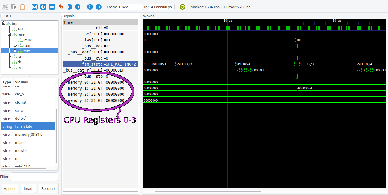
The rom module contains the SPI Flash bus signals, while the CPU registers are represented as memory(x) under the ra, rb, and rc read / write ports.
You can see that the spi_rom.py module simulates reading values from an external SPI Flash chip, and that r1 gets set to 0x4 after the first instruction while the program counter remains at zero. If you look at the cpu_loop.vcd file, you should see the same general signals, but with many fewer clock cycles between each instruction since the simulated rom.py module does not simulate each transaction on the SPI bus.
You can also see that there is no csr submodule in the gtkwave view of the simulation output. That’s what the warnings were about earlier; when you directly modify a submodule’s signal from a parent module, the submodule gets “flattened” into the parent module when the design is built. It’s not a big deal, but it can make the debugging output a little bit less organized.
Generating RISC-V Compliance Test Programs
Now that we’ve got a format which can run machine code and verify register values at a specific times during the program’s execution, we can set up a process to auto-generate test program images for the official RV32I compliance tests.
We can check whether the tests pass or not by observing the state of their registers when the program finishes running: we can set things up so that they set a predefined value in one register when they complete, and a “pass / fail” indication in another. I didn’t end up doing anything sophisticated to detect when a test finishes; I just set them to go into an infinite loop when they finish and made the test program run for 2-3x the number of instructions in the final ROM image.
If you look at the RISC-V compliance tests’ repository, you’ll see that the tests are mostly set up to run in a general-purpose RISC-V simulator, which means that we’ll need to build and run the code in a non-standard way. The assembly code files are in the riscv-test-suite/rv32i/src/ directory, and the supporting header files are in riscv-test-env/.
I made a tests/ directory to store test code, and a tests/rv32i_compliance/ subdirectory to store the compliance test code. I copied all of the *.S source files into that subdirectory, as well as the following files from riscv-test-env/:
riscv_test_macros.htest_macros.hencoding.h(this file should go one directory up, undertests/)p/riscv_test.h
We’ll also need a link.ld linker script to define the basic memory layout when we build each assembly file. There’s nothing fancy here, just the core memory sections with 1MB of ROM and 4KB of RAM:
/* Linker script for a minimal simulated RV32I RISC-V CPU */
OUTPUT_ARCH( "riscv" )
ENTRY( _start )

MEMORY
{
  ROM   (rx)  : ORIGIN = 0x00000000, LENGTH = 1M
  RAM   (rwx) : ORIGIN = 0x20000000, LENGTH = 4K
}

SECTIONS
{
  __stack_size = DEFINED(__stack_size) ? __stack_size : 128;

  .text :
  {
    KEEP (*(SORT_NONE(.reset_handler)))
    KEEP (*(SORT_NONE(.vector_table)))
    *(.rodata .rodata.*)
    *(.srodata .srodata.*)
    *(.text .text.*)
    *(.tohost .tohost.*)
  } >ROM

  . = ALIGN(4);

  PROVIDE (__etext = .);
  PROVIDE (_etext = .);
  PROVIDE (etext = .);

  _sidata = .;
  .data : AT( _sidata )
  {
    . = . + 4;
    _sdata = .;
    *(.rdata)
    *(.data .data.*)
    *(.sdata .sdata.*)
    . = ALIGN(4);
    _edata = .;
  } >RAM

  PROVIDE( _edata = . );
  PROVIDE( edata = . );
  PROVIDE( _fbss = . );
  PROVIDE( __bss_start = . );

  .bss :
  {
    _sbss = .;
    *(.sbss*)
    *(.bss .bss.*)
    *(COMMON)
    . = ALIGN(4);
    _ebss = .;
  } >RAM

  . = ALIGN(8);
  PROVIDE( _end = . );
  PROVIDE( end = . );

  .stack ORIGIN(RAM) + LENGTH(RAM) - __stack_size :
  {
    PROVIDE( _heap_end = . );
    . = __stack_size;
    PROVIDE( _sp = . );
  } >RAM
}
The reset_handler and vector_table sections at the start of .text are not required for the compliance tests, but they will be used later when we write our own C programs.
Next, there are two “client” header files with macros that we need to fill in to work with our platform. You can find examples of these files under the various platform directories in riscv-target/[...]/. First up is compliance_test.h:
// RISC-V Compliance Test Header File

#ifndef _COMPLIANCE_TEST_H
#define _COMPLIANCE_TEST_H

#include "riscv_test.h"

// Use a similar 'TEST_PASSFAIL' macro to
// the one in 'riscv-tests' for now.
#undef RVTEST_PASS
#define RVTEST_PASS              \
        fence;                   \
        li a7, 93;               \
        li a0, 0;                \
        j pass;

#undef RVTEST_FAIL
#define RVTEST_FAIL              \
        fence;                   \
        li a7, 93;               \
        li a0, 0xBAD;            \
        j fail;

#define RV_COMPLIANCE_HALT       \
  pass:                          \
    RVTEST_PASS                  \
  fail:                          \
    RVTEST_FAIL;                 \

#define RV_COMPLIANCE_RV32M      \
  RVTEST_RV32M                   \

#define RV_COMPLIANCE_CODE_BEGIN \
  RVTEST_CODE_BEGIN              \

#define RV_COMPLIANCE_CODE_END   \
  RVTEST_CODE_END                \

#define RV_COMPLIANCE_DATA_BEGIN \
  RVTEST_DATA_BEGIN              \

#define RV_COMPLIANCE_DATA_END   \
  RVTEST_DATA_END                \

#endif
I ended up using the same sort of pass / fail macros as the deprecated riscv-tests repository which these compliance tests have superceded. Once the program finishes, it goes into an infinite loop which sets a7/r17 to a constant value and a0/r10 to a value indicating a passing or failing result.
The second header file that we need to provide is called compliance_io.h:
#ifndef _COMPLIANCE_IO_H
#define _COMPLIANCE_IO_H

// No I/O is available yet.
#define RVTEST_IO_INIT
#define RVTEST_IO_WRITE_STR( _R, _STR )
#define RVTEST_IO_CHECK()
// No floating point units are available.
#define RVTEST_IO_ASSERT_SFPR_EQ( _F, _R, _I )
#define RVTEST_IO_ASSERT_DFPR_EQ( _D, _R, _I )

// Assert that a general-purpose register has a specified value.
// Use the 'TEST_CASE' logic from 'riscv-tests'.
#define RVTEST_IO_ASSERT_GPR_EQ( _G, _R, _I ) \
  li  _G, MASK_XLEN( _I );                    \
  bne _R, _G, fail;

#endif
I left the actual I/O macros un-implemented, and made the “assert equals” macro jump to the fail label if the values are not equal. Finally, there’s a Makefile which builds an object file for each compliance test:
# GCC toolchain programs.
CC = riscv32-unknown-elf-gcc
OD = riscv32-unknown-elf-objdump

# Assembly directives.
# Don't perform optimizations.
ASFLAGS += -O0
# Report all warnings.
ASFLAGS += -Wall
# Just the core RV32I ISA.
ASFLAGS += -march=rv32i
# No extra startup code.
ASFLAGS += -nostartfiles
ASFLAGS += -nostdlib
ASFLAGS += --specs=nosys.specs
ASFLAGS += -Wl,-Tlink.ld

# Source files.
SRC  = ./I-ADD-01.S
SRC += ./I-ADDI-01.S
SRC += ./I-AND-01.S
SRC += ./I-ANDI-01.S
SRC += ./I-AUIPC-01.S
SRC += ./I-BEQ-01.S
SRC += ./I-BGE-01.S
SRC += ./I-BGEU-01.S
SRC += ./I-BLT-01.S
SRC += ./I-BLTU-01.S
SRC += ./I-BNE-01.S
SRC += ./I-DELAY_SLOTS-01.S
SRC += ./I-EBREAK-01.S
SRC += ./I-ECALL-01.S
SRC += ./I-ENDIANESS-01.S
SRC += ./I-IO-01.S
SRC += ./I-JAL-01.S
SRC += ./I-JALR-01.S
SRC += ./I-LB-01.S
SRC += ./I-LBU-01.S
SRC += ./I-LH-01.S
SRC += ./I-LHU-01.S
SRC += ./I-LW-01.S
SRC += ./I-LUI-01.S
SRC += ./I-MISALIGN_JMP-01.S
SRC += ./I-MISALIGN_LDST-01.S
SRC += ./I-NOP-01.S
SRC += ./I-OR-01.S
SRC += ./I-ORI-01.S
SRC += ./I-RF_size-01.S
SRC += ./I-RF_width-01.S
SRC += ./I-RF_x0-01.S
SRC += ./I-SB-01.S
SRC += ./I-SH-01.S
SRC += ./I-SW-01.S
SRC += ./I-SLL-01.S
SRC += ./I-SLLI-01.S
SRC += ./I-SLT-01.S
SRC += ./I-SLTI-01.S
SRC += ./I-SLTIU-01.S
SRC += ./I-SLTU-01.S
SRC += ./I-SRA-01.S
SRC += ./I-SRAI-01.S
SRC += ./I-SRL-01.S
SRC += ./I-SRLI-01.S
SRC += ./I-SUB-01.S
SRC += ./I-XOR-01.S
SRC += ./I-XORI-01.S

# Binary images to build.
OBJS = $(SRC:.S=.o)

# Default rule to build all test files.
.PHONY: all
all: $(OBJS)

# Rule to assemble assembly files.
%.o: %.S
	$(CC) -x assembler-with-cpp $(ASFLAGS) $< -o $@

# Rule to clear out generated build files.
.PHONY: clean
clean:
	rm -f $(OBJS)
If you run make with the RISC-V GNU toolchain installed, it should create a .o file to match each .S file. You can see the raw machine code in those files using objdump -s:
> riscv32-unknown-elf-objdump -s I-ADD-01.o

I-ADD-01.o:     file format elf32-littleriscv

Contents of section .text:
 0000 6f008004 732f2034 930f8000 630aff03  o...s/ 4....c...
 0010 930f9000 6306ff03 930fb000 6302ff03  ....c.......c...
 0020 170f0000 130f0ffe 63040f00 67000f00  ........c...g...
 0030 732f2034 63540f00 6f004000 93e19153  s/ 4cT..o.@....S
[etc...]
Now we just need to write a script to parse that sort of output into Python test programs with starting ROM and RAM values, one for each .o file. I put this in a tests/gen_tests.py file. First, there’s a helper method to generate an array of 32-bit words from a section of data in the object file:
import os
import subprocess
import sys

od = 'riscv32-unknown-elf-objdump'
test_path = "%s/"%( os.path.dirname( sys.argv[ 0 ] ) )

# Helper method to get raw hex out of an object file memory section
# This basically returns the compiled machine code for one
# of the RISC-V assembly test files.
def get_section_hex( op, sect, in_dir ):
  hdump = subprocess.run( [ od, '-s', '-j', sect,
                            './%s/%s/%s'
                            %( test_path, in_dir, op ) ],
                          stdout = subprocess.PIPE
                        ).stdout.decode( 'utf-8' )
  hexl = []
  hls = hdump.split( '\n' )[ 4: ]
  for l in hls:
    hl = l.strip()
    while '  ' in hl:
      hl = hl.replace( '  ', ' ' )
    toks = hl.split( ' ' )
    if len( toks ) < 6:
      break
    hexl.append( '0x%s'%toks[ 1 ].upper() )
    hexl.append( '0x%s'%toks[ 2 ].upper() )
    hexl.append( '0x%s'%toks[ 3 ].upper() )
    hexl.append( '0x%s'%toks[ 4 ].upper() )
  return hexl
It splits the output of a call to objdump by line, then splits each line up by whitespace. Only entries 1-4 are used, since four words of data are printed per line with the address occupying the 0th index. Next is a helper method to write a .py file containing a test program image, given the test name and starting RAM and ROM images:
# Helper method to write a Python file containing a simulated ROM
# test image and testbench condition to verify that it ran correclty.
def write_py_tests( op, hext, hexd, out_dir ):
  instrs = len( hext )
  opp = ''
  opn = op.upper() + ' compliance'
  while len( opp ) < ( 13 - len( op ) ):
    opp = opp + ' '
  py_fn = './%s/%s/rv32i_%s.py'%( test_path, out_dir, op )
  with open( py_fn, 'w' ) as py:
    print( 'Generating %s tests...'%op, end = '' )
    # Write imports and headers.
    py.write( 'from nmigen import *\r\n'
              'from rom import *\r\n'
              '\r\n'
              '###########################################\r\n'
              '# rv32ui %s instruction tests: %s#\r\n'
              '###########################################\r\n'
              '\r\n'%( op.upper(), opp ) )
    # Write the ROM image.
    py.write( '# Simulated ROM image:\r\n'
              '%s_rom = rom_img( ['%op )
    for x in range( len( hext ) ):
      if ( x % 4 ) == 0:
        py.write( '\r\n  ' )
      py.write( '%s'%hext[ x ] )
      if x < ( len( hext ) - 1 ):
        py.write( ', ' )
    py.write( '\r\n] )\r\n' )
    # Write the inirialized RAM values.
    py.write( '\r\n# Simulated initialized RAM image:\r\n'
              '%s_ram = ram_img( ['%op )
    for x in range( len( hexd ) ):
      if ( x % 4 ) == 0:
        py.write( '\r\n  ' )
      py.write( '%s'%hexd[ x ] )
      if x < ( len( hexd ) - 1 ):
        py.write( ', ' )
    py.write( '\r\n] )\r\n' )
    # Run most tests for 2x the number of instructions to account
    # for jumps, except for the 'fence' test which uses 3x because
    # it has a long 'prefetcher test' which counts down from 100.
    num_instrs = ( instrs * 3 ) if 'fence' in op else ( instrs * 2 )
    # Write the 'expected' value for the testbench to check
    # after tests finish.
    py.write( "\r\n# Expected 'pass' register values.\r\n"
              "%s_exp = {\r\n"
              "  %d: [ { 'r': 17, 'e': 93 }, { 'r': 10, 'e': 0 } ],"
              "  'end': %d\r\n}\r\n"%( op, num_instrs, num_instrs ) )
    # Write the test struct.
    py.write( "\r\n# Collected test program definition:\r\n%s_test = "
              "[ '%s tests', 'cpu_%s', %s_rom, %s_ram, %s_exp ]"
              %( op, opn, op, op, op, op ) )
  print( "Done!" )
Finally, there’s some logic to run make clean && make and call the above methods once for each compliance test file:
# Ensure that the test ROM directories exists.
if not os.path.exists( './%s/test_roms'%test_path ):
  os.makedirs( './%s/test_roms'%test_path )
# Run 'make clean && make' to re-compile the files.
subprocess.run( [ 'make', 'clean' ],
                cwd = './%s/rv32i_compliance/'%test_path )
subprocess.run( [ 'make' ],
                cwd = './%s/rv32i_compliance/'%test_path )
# Process all compiled test files.
for fn in os.listdir( './%s/rv32i_compliance'%test_path ):
  if fn[ -1 ] == 'o':
    op = fn[ :-2 ]
    # Get machine code instructions for the operation's tests.
    hext = get_section_hex( '%s.o'%op, '.text', 'rv32i_compliance' )
    # Get initialized RAM data for the operation's tests.
    hexd = get_section_hex( '%s.o'%op, '.data', 'rv32i_compliance' )
    # Write a Python file with the test program image.
    write_py_tests( op[ 2 : -3 ].lower(), hext, hexd, 'test_roms' )
If you run that gen_tests.py file, it should create a test_roms/ directory full of Python files which contain test program images. For example, rv32i_add.py might look something like this:
from nmigen import *
from rom import *

###########################################
# rv32ui ADD instruction tests:           #
###########################################

# Simulated ROM image:
add_rom = rom_img( [
  0x6F008004, 0x732F2034, 0x930F8000, 0x630AFF03,
  [...]
  0x00000000, 0x00000000, 0x00000000, 0x00000000
] )

# Simulated initialized RAM image:
add_ram = ram_img( [
  0x00000000, 0x00000000, 0x00000000, 0x00000000,
  [...]
  0x00000000, 0x00000000, 0x00000000, 0x00000000
] )

# Expected 'pass' register values.
add_exp = {
  768: [ { 'r': 17, 'e': 93 }, { 'r': 10, 'e': 0 } ],  'end': 768
}

# Collected test program definition:
add_test = [ 'ADD compliance tests', 'cpu_add', add_rom, add_ram, add_exp ]
And you can run each test by importing it and calling cpu_sim with it in cpu.py:
from tests.test_roms.rv32i_add import *
from tests.test_roms.rv32i_addi import *
from tests.test_roms.rv32i_and import *
from tests.test_roms.rv32i_andi import *
[...etc...]

# 'main' method to run a basic testbench.
if __name__ == "__main__":
  # Run testbench simulations.
  with warnings.catch_warnings():
    warnings.filterwarnings( "ignore", category = DriverConflict )

    print( '--- CPU Tests ---' )
    # Simulate the 'infinite loop' ROM to screen for syntax errors.
    cpu_sim( loop_test )
    cpu_spi_sim( loop_test )
    cpu_sim( ram_pc_test )
    cpu_spi_sim( ram_pc_test )
    cpu_sim( add_test )
    cpu_sim( addi_test )
    cpu_sim( and_test )
    cpu_sim( andi_test )
    [...etc...]

    # Done; print results.
    print( "CPU Tests: %d Passed, %d Failed"%( p, f ) )
You should see the tests pass, like before:
--- CPU Tests ---
START running 'inifinite loop test' program:
  PASS: pc  == 0x00000000 after 0 operations
  PASS: pc  == 0x00000000 after 1 operations
  [...]
  PASS: r09 == 0x00000123 after 21 operations
DONE running run from RAM test: executed 22 instructions
START running 'ADD compliance tests' program:
  PASS: r17 == 0x0000005D after 768 operations
  PASS: r10 == 0x00000000 after 768 operations
DONE running ADD compliance tests: executed 768 instructions
START running 'ADDI compliance tests' program:
  PASS: r17 == 0x0000005D after 768 operations
  PASS: r10 == 0x00000000 after 768 operations
DONE running ADDI compliance tests: executed 768 instructions
START running 'AND compliance tests' program:
  PASS: r17 == 0x0000005D after 768 operations
  PASS: r10 == 0x00000000 after 768 operations
DONE running AND compliance tests: executed 768 instructions
START running 'ANDI compliance tests' program:
  PASS: r17 == 0x0000005D after 768 operations
  PASS: r10 == 0x00000000 after 768 operations
DONE running ANDI compliance tests: executed 768 instructions
CPU Tests: 46 Passed, 0 Failed
If you run the rest of the compliance tests, they should all pass. You can also compare the source code to the waveform results; it takes much longer than just checking that they all finished without any test failures, but it gives you a better insight to how the test runs. You can use objdump -d to print a program’s disassembly as a list of instructions, one to each line. For example, take a look at the ADD instruction’s compliance test:
$ riscv32-unknown-elf-objdump -d I-ADD-01.o

I-ADD-01.o:     file format elf32-littleriscv

Disassembly of section .text:

00000000 <_start>:
   0:	0480006f          	j	48 <reset_vector>

00000004 <trap_vector>:
   4:	34202f73          	csrr	t5,mcause
   8:	00800f93          	li	t6,8
   c:	03ff0a63          	beq	t5,t6,40 <write_tohost>
  10:	00900f93          	li	t6,9
  [...etc...]

00000048 <reset_vector>:
  48:	f1402573          	csrr	a0,mhartid
  4c:	00051063          	bnez	a0,4c <reset_vector+0x4>
  50:	00000297          	auipc	t0,0x0
  54:	01028293          	addi	t0,t0,16 # 60 <reset_vector+0x18>
  58:	30529073          	csrw	mtvec,t0
  5c:	18005073          	csrwi	satp,0
  60:	00000297          	auipc	t0,0x0
  [...etc...]
If you look at address 0x08, you can see that the LI “Load Integer” pseudo-operation gets implemented as an ADDI “Add Immediate” instruction when it loads a small value. The opcode bits are 0b0010011, the destination register is set to 0b11111, the funct3 bits are set to 0b000, the source register is set to 0b00000, and the immediate value is set to 0x008. If you compare those values to the table of valid RV32I instructions, you can see that it translates to r31 = r0 + 8. You can see how the CPU registers are usually named near the top of the “RISC-V Assembly Programmer’s Manual”: x0 (r0) is the special read-only register which always returns zero, and x31 (r31) is called t6 for “temporary register 6”.
You can go through the same process of parsing individual instructions to check the other values, but you can also see that the disassembler automatically converts each word to a human-readable instruction on the right side of the output. And if you look at the cpu_add.vcd waveform file which was generated by our simulating the first few compliance tests earlier, you should see that the program counter and register values match the disassembly:
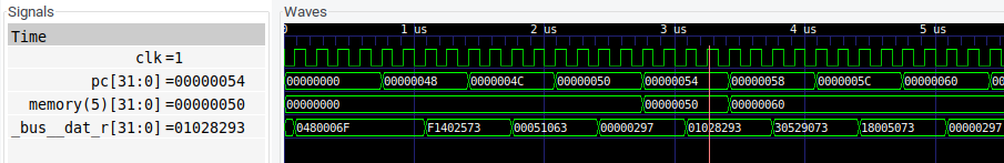
The first few “ADD” compliance test instructions seem to do what they should.
If you look back at the assembly programmer’s manual, you’ll see that t0 (“temporary register 0”) corresponds to register #5 in the CPU. And given the disassembly above, we can expect the first instruction to jump to the reset handler at 0x48, followed by a CSR and branch instruction. At address 0x50, the AUIPC instruction is used to store the current program counter’s value in t0, after which it will add 16 (0x10) to that same value. You can see in the simulation above that the test program does that, and you can also see that the dat_r outputs on the imux instruction Wishbone bus contain the machine code instructions indicated in the disassembly.
You can try running all of the RV32I compliance tests listed in the previous Makefile this way, and they should all pass. That means that we now have a mostly-compliant RISC-V CPU! No rest for the weary, though: a CPU isn’t very useful without configurable inputs and outputs, so let’s keep moving.
Peripherals: Pins, PWM, and GPIO
Now that we have some confidence that our CPU works, let’s implement the typical “hello world” task of blinking an LED. To do that, we’ll need a way to control the FPGA’s I/O pins. If you remember from my last post on nMigen, we can retrieve resources like Pins from the platform object using platform.request(name, index). But we can only request each resource once, so in addition to the peripheral modules themselves, we’ll also need a “pin multiplexer” module to keep track of the resources and configure which pins should connect to which peripherals.
Since nMigen is such a young framework, there is not always a lot of guidance on the “right” way to do things like access GPIO pins depending on a board file. I haven’t quite figured out how to use the Connector objects which the official board files seem to use, so I wrote a non-standard upduino.py board file for an Upduino V2 board. I replaced the LED pin Resources with objects generated from a PINS array of valid pin numbers:
from nmigen.build import *
from nmigen.vendor.lattice_ice40 import *
from nmigen_boards.resources import *

import os
import subprocess

__all__ = ["PINS", "UpduinoPlatform"]

PINS = [ 2, 3, 4, 9, 11, 13, 18, 19, 21, 23, 25, 26, 27, 31, 32,
         34, 35, 36, 37, 38, 39, 40, 41, 42, 43, 44, 45, 46, 47, 48 ]

class UpduinoPlatform(LatticeICE40Platform):
    device      = "iCE40UP5K"
    package     = "SG48"
    default_clk = "SB_HFOSC"
    hfosc_div   = 3
    resources   = [
        *LEDResources(pins="39 40 41", invert=True,
                      attrs=Attrs(IO_STANDARD="SB_LVCMOS")),

        *SPIFlashResources(0,
            cs="16", clk="15", miso="17", mosi="14",
            attrs=Attrs(IO_STANDARD="SB_LVCMOS")
        ),

        # Solder pin 12 to the adjacent 'J8' osc_out pin to enable.
        Resource("clk12", 0, Pins("12", dir="i"),
                 Clock(12e6), Attrs(IO_STANDARD="SB_LVCMOS")),
    ]

    for i in PINS:
      resources.append(Resource("gpio", i, Pins("%d"%i, dir="io"),
               Attrs(IO_STANDARD = "SB_LVCMOS")))

    connectors  = [
        # "Left" row of header pins (JP5 on the schematic)
        Connector("j", 0, "- - 23 25 26 27 32 35 31 37 34 43 36 42 38 28"),
        # "Right" row of header pins (JP6 on the schematic)
        Connector("j", 1, "12 21 13 19 18 11 9 6 44 4 3 48 45 47 46 2")
    ]

    def toolchain_program(self, products, name):
        iceprog = os.environ.get("ICEPROG", "iceprog")
        with products.extract("{}.bin".format(name)) as bitstream_filename:
            subprocess.check_call([iceprog, bitstream_filename])


if __name__ == "__main__":
    from nmigen_boards.test.blinky import *
    UpduinoPlatform().build(Blinky(), do_program=True)
This looks very similar to most other nMigen board files, except for the PINS array and corresponding gpio resources. I would like to come up with a better way of doing this so that you don’t need to use a modified board file, but this works for now.
GPIO Peripheral
One easy way to create peripherals for an FPGA design is to implement a series of “registers” which can be accessed using ordinary load and store instructions. And instead of a large Memory object, the register bitfields can be assembled or parsed on-the-fly from smaller peripheral Signals.
For a minimal GPIO peripheral, we can define two bits for each pin: one to set the input / output direction, and one to represent the current high / low value on the pin. We can also initialize the same sort of Wishbone bus Interface object that the other memory modules use, to allow access via the CPU’s normal load / store instructions:
from nmigen import *
from nmigen.lib.io import *
from nmigen.back.pysim import *

from nmigen_soc.wishbone import *
from nmigen_soc.memory import *

from isa import *
from upduino import *

##################################
# GPIO interface: allow I/O pins #
# to be written and read.        #
##################################
class GPIO( Elaboratable, Interface ):
  def __init__( self ):
    # Initialize wishbone bus interface to support up to 64 pins.
    # Each pin has two bits, so there are 16 pins per register:
    # * 0: value. Contains the current I/O pin value. Only writable
    #      in output mode. Writes to input pins are ignored.
    #      (But they might get applied when the direction switches?)
    # * 1: direction. When set to '0', the pin is in input mode and
    #      its output is disabled. When set to '1', it is in output
    #      mode and the value in bit 0 will be reflected on the pin.
    #
    # iCE40s don't have programmable pulling resistors, so...
    # not many options here. You get an I, and you get an O.
    Interface.__init__( self, addr_width = 5, data_width = 32 )
    self.memory_map = MemoryMap( addr_width = self.addr_width,
                                 data_width = self.data_width,
                                 alignment = 0 )
    # Backing data store. A 'Memory' would be smaller, but
    # the 'pin multiplexer' peripheral needs parallel access.
    self.p = Array(
      Signal( 2, reset = 0, name = "gpio_%d"%i ) if i in PINS else None
      for i in range( 49 ) )
The runtime logic can also be quite simple. Besides mediating the Wishbone bus transactions, there’s a switch case that determines which 32-bit register should be accessed based on the bus address. With two bits of data per pin, that means each register can hold information about up to 16 pins:
  def elaborate( self, platform ):
    m = Module()

    # Read bits default to 0. Bus signals follow 'cyc'.
    m.d.comb += [
      self.dat_r.eq( 0 ),
      self.stb.eq( self.cyc )
    ]
    m.d.sync += self.ack.eq( self.cyc )

    # Switch case to select the currently-addressed register.
    # This peripheral must be accessed with a word-aligned address.
    with m.Switch( self.adr ):
      for i in range( 4 ):
        with m.Case( i * 4 ):
          # Logic for each of the register's 16 possible pins,
          # ignoring ones that aren't in the 'PINS' array.
          for j in range( 16 ):
            pnum = ( i * 16 ) + j
            if pnum in PINS:
              # Read logic: populate 'value' and 'direction' bits.
              m.d.comb += self.dat_r.bit_select( j * 2, 2 ).eq(
                self.p[ pnum ] )
              # Write logic: if this bus is selected and writes
              # are enabled, set 'value' and 'direction' bits.
              with m.If( ( self.we == 1 ) & ( self.cyc == 1 ) ):
                m.d.sync += self.p[ pnum ].eq(
                  self.dat_w.bit_select( j * 2, 2 ) )

    # (End of GPIO peripheral module definition)
    return m
I chose to use the FPGA pin number as an index for each GPIO pin. This results in sparsely-packed registers, because some pins are reserved for debugging, the power supply, or other functionality like SPI Flash. You should be very careful to avoid re-programming the SPI Flash pins, because you can brick cheap iCE40 boards like the Upduino if you corrupt that communication channel. To prevent that from happening, I ommitted pins #14-17 in the PINS array.
The bits for pin numbers which are not included in the PINS array will act as reserved read-only bits which always return zero. You could make a more efficient design with fewer registers by packing the pins in as tightly as possible, but I figured that this educational project is not important enough to merit a whole new pin-naming convention, so I used index numbers based on the FPGA pakaging to avoid confusion.
Sadly, I haven’t written testbenches for any of these peripheral modules yet. That is bad practice, but as we’ll see in a little bit, it’s still possible to test the functionality by simulating a C program which accesses these peripheral registers.
PWM Peripheral
The LEDs included on most iCE40UP5K boards tend to be very bright, and there’s not much point in setting up a multiplexer for pin / peripheral mappings if we only have one GPIO peripheral available. So let’s also add a few PWM peripherals to provide Pulse-Width Modulation outputs for dimming and brightening LEDs rather than just toggling them between ‘on’ and ‘off’.
I decided to make this peripheral very simple and small, so it doesn’t have many features. It maintains an 8-bit counter, which constantly increments in the background. It also has a 1-bit “output” value which gets sent to the connected pin, and an 8-bit “compare” value which can be read and written in a peripheral register:
from nmigen import *

from nmigen_soc.wishbone import *
from nmigen_soc.memory import *

################################################
# PWM "Pulse Width Modulation" peripheral      #
# Produces a PWM output based on an 8-bit      #
# value that constantly counts up.             #
# When the counter is less than the 'compare'  #
# value, the output is 1. When it reaches the  #
# max value of 0xFF, it resets. If 'compare'   #
# is 0, the output is effectively disabled.    #
################################################

# Peripheral register offset (there's only one, so...zero)
# Bits 0-8:  'compare' value.
PWM_CR = 0

class PWM( Elaboratable, Interface ):
  def __init__( self ):
    # Initialize wishbone bus interface for peripheral registers.
    # This seems sort of pointless with only one register, but
    # it lets the peripheral be added to the wider memory map.
    Interface.__init__( self, addr_width = 1, data_width = 32 )
    self.memory_map = MemoryMap( addr_width = self.addr_width,
                                 data_width = self.data_width,
                                 alignment = 0 )

    # Peripheral signals. Use 8 bits to allow duty cycles
    # to be set with a granularity of ~0.4%
    self.compare = Signal( 8, reset = 0 )
    self.count   = Signal( 8, reset = 0 )
    # Current output value.
    self.o       = Signal( 1,  reset = 0 )
The runtime logic asserts the output value when the counter is less than the “compare” value That is the opposite of what you might expect, because the on-board LEDs are wired such that a “high” output turns the LEDs off and a “low” output turns them on. You might want to add a “direction” bit which can be set in the one available peripheral register, but I’ll leave that as an exercise to the reader:
  def elaborate( self, platform ):
    m = Module()

    m.d.comb += [
      # Set the pin output value.
      # TODO: This is backwards, because the LEDs are wired backwards
      # on most iCE40 boards. It should be '<', not '>='.
      self.o.eq( self.count >= self.compare ),
      # Peripheral bus signals follow 'cyc'.
      self.stb.eq( self.cyc )
    ]
    m.d.sync += [
      # Increment the counter.
      self.count.eq( self.count + 1 ),
      # Peripheral bus signals follow 'cyc'.
      self.ack.eq( self.cyc )
    ]

    # There's only one peripheral register, so we don't really need
    # a switch case. Only address 0 is valid.
    with m.If( self.adr == 0 ):
      # The "compare" value is located in the register's 8 LSbits.
      m.d.comb += self.dat_r.eq( self.compare )
      with m.If( self.we & self.cyc ):
        m.d.sync += self.compare.eq( self.dat_w[ :8 ] )

    return m
This logic will update the peripheral’s o (“output”) value, which the pin multiplexer will forward to the appropriate pin(s).
Pin Multiplexer
Now that we have two types of peripherals which can make use of an I/O pin, we need a module to mediate access to the hardware resources. I set up a gpio_mux.py module to define peripheral registers with 4 bits of data per pin. Depending on that “function select” value, the module will forward signals between the pin Resource object and one of the many supported peripherals:
from nmigen import *
from nmigen.lib.io import *
from nmigen.back.pysim import *

from nmigen_soc.wishbone import *
from nmigen_soc.memory import *

from isa import *
from upduino import *

##########################################
# GPIO multiplexer interface:            #
# Map I/O pins to different peripherals. #
# Each pin gets 4 bits:                  #
# * 0x0: GPIO (default)                  #
# * 0xN: PWM peripheral #(N)             #
##########################################

# Number of PWM peripherals to expect.
PWM_PERIPHS = 3

# Dummy GPIO pin class for simulations.
class DummyGPIO():
  def __init__( self, name ):
    self.o  = Signal( name = "%s_o"%name )
    self.i  = Signal( name = "%s_i"%name )
    self.oe = Signal( name = "%s_oe"%name )

class GPIO_Mux( Elaboratable, Interface ):
  def __init__( self, periphs ):
    # Wishbone interface: address <=64 pins, 4 bits per pin.
    # The bus is 32 bits wide for compatibility, so 8 pins per word.
    Interface.__init__( self, addr_width = 6, data_width = 32 )
    self.memory_map = MemoryMap( addr_width = self.addr_width,
                                 data_width = self.data_width,
                                 alignment = 0 )
    # Backing data store for QFN48 pins. A 'Memory' would be more
    # efficient, but the module must access each field in parallel.
    self.pin_mux = Array(
      Signal( 4, reset = 0, name = "pin_func_%d"%i ) if i in PINS else None
      for i in range( 49 ) )

    # Unpack peripheral modules (passed in from 'rvmem.py' module).
    self.gpio = periphs[ 0 ]
    self.pwm = []
    pind = 1
    for i in range( PWM_PERIPHS ):
      self.pwm.append( periphs[ pind ] )
      pind += 1
There’s a DummyGPIO object which acts similarly to the “dummy” pin and SPI resources in spi_rom.py. It has the same basic attributes as a pin Resource: o (“output”), i (“input”), and oe (“output enable”). Then, besides the Array of 4-bit “function select” signals, there are records for each of the peripheral submodules which must be passed into the __init__ method.
For the runtime logic, first the module needs to request the actual pin Resources from the platform object if the design is being built, or define DummyGPIO objects if it is being simulated, and handle the Wishbone bus signals:
  def elaborate( self, platform ):
    m = Module()

    # Set up I/O pin resources.
    if platform is None:
      self.p = Array(
        DummyGPIO( "pin_%d"%i ) if i in PINS else None
        for i in range( max( PINS ) + 1 ) )
    else:
      self.p = Array(
        platform.request( "gpio", i ) if i in PINS else None
        for i in range( max( PINS ) + 1 ) )

    # Read bits default to 0. Bus signals follow 'cyc'.
    m.d.comb += [
      self.dat_r.eq( 0 ),
      self.stb.eq( self.cyc ),
    ]
    m.d.sync +=  self.ack.eq( self.cyc )
Then, there’s the read / write logic for the peripheral registers. This works just like it does in the GPIO and PWM peripherals above, to allow software to access the 4-bit “function select” values with 8 pins per 32-bit register:
    # Switch case to read/write the currently-addressed register.
    # This peripheral must be accessed with a word-aligned address.
    with m.Switch( self.adr ):
      # 49 pin addresses (0-48), 8 pins per register, so 7 registers.
      for i in range( 7 ):
        with m.Case( i * 4 ):
          # Read logic for valid pins (each has 4 bits).
          for j in range( 8 ):
            pnum = ( i * 8 ) + j
            if pnum in PINS:
              m.d.comb += self.dat_r.bit_select( j * 4, 4 ).eq(
                self.pin_mux[ pnum ] )
              # Write logic for valid pins (again, 4 bits each).
              with m.If( ( self.cyc == 1 ) &
                         ( self.we == 1 ) ):
                m.d.sync += self.pin_mux[ pnum ].eq(
                  self.dat_w.bit_select( j * 4, 4 ) )
Finally, there’s the actual pin multiplexing logic. Each pin gets its own switch case, which forwards “input” and “output” values between a pin and its currently-selected peripheral:
    # Pin multiplexing logic.
    for i in range( 49 ):
      if i in PINS:
        pind = 1
        # Each valid pin gets its own switch case, which ferries
        # signals between the selected peripheral and the actual pin.
        with m.Switch( self.pin_mux[ i ] ):
          # GPIO peripheral:
          with m.Case( 0 ):
            # Apply 'value' and 'direction' bits.
            m.d.sync += self.p[ i ].oe.eq( self.gpio.p[ i ][ 1 ] )
            # Read or write, depending on the 'direction' bit.
            with m.If( self.gpio.p[ i ][ 1 ] == 0 ):
              m.d.sync += self.gpio.p[ i ].bit_select( 0, 1 ) \
                .eq( self.p[ i ].i )
            with m.Else():
              m.d.sync += self.p[ i ].o.eq( self.gpio.p[ i ][ 0 ] )
          # PWM peripherals:
          for j in range( PWM_PERIPHS ):
            with m.Case( pind ):
              # Set pin to output mode, and set its current value.
              m.d.sync += [
                self.p[ i ].oe.eq( 1 ),
                self.p[ i ].o.eq( self.pwm[ j ].o )
              ]
            pind += 1

    # (End of GPIO multiplexer module)
    return m
Now we just need to instantiate these peripheral modules, and add them to the data bus in our rvmem.py “memory multiplexer” module.
Updated Memory Multiplexer
Since our peripherals all implement the same Wishbone bus standard as the RAM and ROM modules, the rvmem.py module doesn’t need many changes to support them. The initialization logic looks very similar to the earlier module:
from nmigen import *
from nmigen.back.pysim import *
from nmigen_soc.wishbone import *
from nmigen_soc.memory import *

from gpio import *
from gpio_mux import *
from pwm import *
from ram import *

#############################################################
# "RISC-V Memories" module.                                 #
# This directs memory accesses to the appropriate submodule #
# based on the memory space defined by the 3 MSbs.          #
# (None of this is actually part of the RISC-V spec)        #
# Current memory spaces:                                    #
# *  0x0------- = ROM                                       #
# *  0x2------- = RAM                                       #
# *  0x4------- = Peripherals                               #
# ** 0x4000---- = GPIO pins                                 #
# ** 0x4001---- = Pin : Peripheral multiplexer              #
# ** 0x4002---- = PWM peripherals                           #
# ** 0x40020x-- = PWM peripheral #(x-1)                     #
#############################################################

class RV_Memory( Elaboratable ):
  def __init__( self, rom_module, ram_words ):
    # Memory multiplexers.
    # Data bus multiplexer.
    self.dmux = Decoder( addr_width = 32,
                         data_width = 32,
                         alignment = 0 )
    # Instruction bus multiplexer.
    self.imux = Decoder( addr_width = 32,
                         data_width = 32,
                         alignment = 0 )

    # Add ROM and RAM buses to the data multiplexer.
    self.rom = rom_module
    self.ram = RAM( ram_words )
    self.rom_d = self.rom.new_bus()
    self.ram_d = self.ram.new_bus()
    self.dmux.add( self.rom_d,    addr = 0x00000000 )
    self.dmux.add( self.ram_d,    addr = 0x20000000 )
    # Add peripheral buses to the data multiplexer.
    # GPIO peripheral.
    self.gpio = GPIO()
    self.dmux.add( self.gpio,     addr = 0x40000000 )
    # PWM peripherals.
    self.pwm = []
    p_adr = 0x40020000
    for i in range( PWM_PERIPHS ):
      self.pwm.append( PWM() )
      self.dmux.add( self.pwm[ i ], addr = p_adr )
      p_adr += 0x0100
    # Pin : peripheral multiplexer
    gpio_mux_arr = [ self.gpio ]
    gpio_mux_arr.extend( self.pwm )
    self.gpio_mux = GPIO_Mux( gpio_mux_arr )
    self.dmux.add( self.gpio_mux, addr = 0x40010000 )

    # Add ROM and RAM buses to the instruction multiplexer.
    self.rom_i = self.rom.new_bus()
    self.ram_i = self.ram.new_bus()
    self.imux.add( self.rom_i,    addr = 0x00000000 )
    self.imux.add( self.ram_i,    addr = 0x20000000 )
    # (No peripherals on the instruction bus)
The only difference is the addition of a peripheral memory space starting at 0x40000000 on the data bus. The GPIO peripheral registers go at the base address, and the “pin multiplexer” peripheral goes at 0x40010000. A number of PWM peripherals are also added starting at 0x40020000; the PWM_PERIPHS value from the gpio_mux.py file determines how many.
The runtime logic also looks very similar to what we wrote earlier – the only difference is that it also registers each peripheral as a submodule:
  def elaborate( self, platform ):
    m = Module()
    # Register the multiplexers, peripherals, and memory submodules.
    m.submodules.dmux     = self.dmux
    m.submodules.imux     = self.imux
    m.submodules.rom      = self.rom
    m.submodules.ram      = self.ram
    m.submodules.gpio     = self.gpio
    for i in range( PWM_PERIPHS ):
      setattr( m.submodules, "pwm%i"%i, self.pwm[ i ] )
    m.submodules.gpio_mux = self.gpio_mux

    # Currently, all bus cycles are single-transaction.
    # So set the 'strobe' signals equal to the 'cycle' ones.
    m.d.comb += [
      self.dmux.bus.stb.eq( self.dmux.bus.cyc ),
      self.imux.bus.stb.eq( self.imux.bus.cyc )
    ]

    return m
And that’s it! We don’t need to make any changes to the CPU logic, because the peripheral registers will be accessed using ordinary memory access operations.
Code: Writing and Running C Code on Your CPU
Okay, so we’ve got a microcontroller CPU – let’s write some code for it! I created a new tests/hw_tests/ directory to store test programs that will be run on the FPGA hardware. And in that directory, I added a common/ subdirectory to hold shared files which are used by more than one test program.
Shared Program Files
First, copy the tests/encoding.h and tests/rv32i_compliance/link.ld files into tests/hw_tests/common/. We can use the linker script and basic RISC-V encodings from the compliance tests for a basic C program. Then, we’ll need a common/start.S assembly file to hold the reset handler and vector table:
#include "encoding.h"

/* Reset handler. */
.global _start
.type _start, %object
.section .reset_handler,"a",%progbits
_start:
  // Ensure that interrupts are disabled.
  csrrci x0, mstatus, MSTATUS_MIE
  // Set the stack pointer address.
  la sp, _sp
  // Set the default vector table address.
  la t0, vtable
  csrrw x0, mtvec, t0
  // Set vectored interrupt mode.
  csrrsi x0, mtvec, 0x1
  // Call main(0, 0) in case 'argc' and 'argv' are present.
  li a0, 0
  li a1, 1
  call main


/*
 * Main vector table entries.
 * Hold entries for supported vectored exception and interrupts.
 * TODO: Have the CPU jump to the addresses instead of running them.
 */
.global vtable
.type vtable, %object
.section .vector_table,"a",%progbits
vtable:
  // 0: Misaligned instruction address fault.
  J trap_imis
  .word 0
  .word 0
  // 3: Breakpoint trap.
  J trap_ebreak
  // 4: Misaligned load address fault.
  J trap_lmis
  .word 0
  // 6: Misaligned store address fault.
  J trap_smis
  .word 0
  .word 0
  .word 0
  .word 0
  // 11: Environment call from M-mode trap.
  J trap_ecall

  /*
   * Weak aliases to point each exception hadnler to the
   * 'default_interrupt_handler', unless the application defines
   * a function with the same name to override the reference.
   */
  .weak trap_imis
  .set  trap_imis,default_interrupt_handler
  .weak trap_ebreak
  .set  trap_ebreak,default_interrupt_handler
  .weak trap_lmis
  .set  trap_lmis,default_interrupt_handler
  .weak trap_smis
  .set  trap_smis,default_interrupt_handler
  .weak trap_ecall
  .set  trap_ecall,default_interrupt_handler

/*
 * A 'default' interrupt handler, in case an interrupt triggers
 * without a handler being defined.
 */
.section .text.default_interrupt_handler,"ax",%progbits
default_interrupt_handler:
    default_interrupt_loop:
      j default_interrupt_loop
Remember from the “CPU” section that there are two types of trap-handling modes; I chose to use the “vectored” mode which lets each type of trap jump to a different function. These minimal tests programs shouldn’t trigger any traps, but that’s what the csrrsi x0, mtvec, 0x1 command does: it sets the “mode” bit in the MTVEC CSR, whose upper 30 bits hold the vector table’s word-aligned starting address.
Moving on, we’ll also need a cpu.h device header file with definitions for the peripheral register addresses and bitfields:
#ifndef __CPU_DEVICE
#define __CPU_DEVICE

#include <stdint.h>

// Device header file:
// GPIO struct: 4 registers, 16 pins per register.
typedef struct
{
  volatile uint32_t P1;
  volatile uint32_t P2;
  volatile uint32_t P3;
  volatile uint32_t P4;
} GPIO_TypeDef;
// GPIO multiplexer strut: 7 registers, 8 pins per register.
typedef struct
{
  volatile uint32_t CFG1;
  volatile uint32_t CFG2;
  volatile uint32_t CFG3;
  volatile uint32_t CFG4;
  volatile uint32_t CFG5;
  volatile uint32_t CFG6;
  volatile uint32_t CFG7;
} IOMUX_TypeDef;
// Pulse Width Modulation struct: only one register.
typedef struct
{
  // "Control register": Holds the 'compare' and 'max' values
  // which determine the PWM duty cycle.
  volatile uint32_t CR;
} PWM_TypeDef;

// Peripheral address definitions
#define GPIO  ( ( GPIO_TypeDef * )  0x40000000 )
#define IOMUX ( ( IOMUX_TypeDef * ) 0x40010000 )
#define PWM1  ( ( PWM_TypeDef * )   0x40020000 )
#define PWM2  ( ( PWM_TypeDef * )   0x40020100 )
#define PWM3  ( ( PWM_TypeDef * )   0x40020200 )

// GPIO pin address offsets.
// (not every pin is an I/O pin)
#define GPIO2_O  ( 4 )
#define GPIO3_O  ( 6 )
#define GPIO4_O  ( 8 )
#define GPIO9_O  ( 18 )
#define GPIO11_O ( 22 )
#define GPIO12_O ( 24 )
#define GPIO13_O ( 26 )
#define GPIO18_O ( 4 )
#define GPIO19_O ( 6 )
#define GPIO21_O ( 10 )
#define GPIO23_O ( 14 )
#define GPIO25_O ( 18 )
#define GPIO26_O ( 20 )
#define GPIO27_O ( 22 )
#define GPIO31_O ( 30 )
#define GPIO32_O ( 0 )
#define GPIO33_O ( 2 )
#define GPIO34_O ( 4 )
#define GPIO35_O ( 6 )
#define GPIO36_O ( 8 )
#define GPIO37_O ( 10 )
#define GPIO38_O ( 12 )
#define GPIO39_O ( 14 )
#define GPIO40_O ( 16 )
#define GPIO41_O ( 18 )
#define GPIO42_O ( 20 )
#define GPIO43_O ( 22 )
#define GPIO44_O ( 24 )
#define GPIO45_O ( 26 )
#define GPIO46_O ( 28 )
#define GPIO47_O ( 30 )
#define GPIO48_O ( 0 )

// GPIO multiplexer pin configuration values.
#define IOMUX_GPIO ( 0x0 )
#define IOMUX_PWM1 ( 0x1 )
#define IOMUX_PWM2 ( 0x2 )
#define IOMUX_PWM3 ( 0x3 )
// GPIO multiplexer pin configuration offsets.
#define IOMUX2_O   ( 8 )
#define IOMUX3_O   ( 12 )
#define IOMUX4_O   ( 16 )
#define IOMUX9_O   ( 4 )
#define IOMUX11_O  ( 12 )
#define IOMUX12_O  ( 16 )
#define IOMUX13_O  ( 20 )
#define IOMUX18_O  ( 8 )
#define IOMUX19_O  ( 12 )
#define IOMUX21_O  ( 20 )
#define IOMUX23_O  ( 28 )
#define IOMUX25_O  ( 4 )
#define IOMUX26_O  ( 8 )
#define IOMUX27_O  ( 12 )
#define IOMUX31_O  ( 28 )
#define IOMUX32_O  ( 0 )
#define IOMUX33_O  ( 4 )
#define IOMUX34_O  ( 8 )
#define IOMUX35_O  ( 12 )
#define IOMUX36_O  ( 16 )
#define IOMUX37_O  ( 20 )
#define IOMUX38_O  ( 24 )
#define IOMUX39_O  ( 28 )
#define IOMUX40_O  ( 0 )
#define IOMUX41_O  ( 4 )
#define IOMUX42_O  ( 8 )
#define IOMUX43_O  ( 12 )
#define IOMUX44_O  ( 16 )
#define IOMUX45_O  ( 20 )
#define IOMUX46_O  ( 24 )
#define IOMUX47_O  ( 28 )
#define IOMUX48_O  ( 0 )

// PWM peripheral control register offsets and masks.
#define PWM_CR_CMP_O ( 0 )
#define PWM_CR_CMP_M ( 0xFF << PWM_CR_CMP_O )

#endif
Now we can write a test program the same way that we would for any other microcontroller.
GPIO Test: Blinking LED
For a simple test program, we only need a main.c source file and a Makefile. I put these “blinking LED” test files in a tests/hw_tests/led_test/ subdirectory. First, the main.c file looks like a normal “hello world” microcontroller program:
// Standard library includes.
#include <stdint.h>
#include <string.h>
// Device header files
#include "encoding.h"
#include "cpu.h"

// Pre-defined memory locations for program initialization.
extern uint32_t _sidata, _sdata, _edata, _sbss, _ebss;
// 'main' method which gets called from the boot code.
int main( void ) {
  // Copy initialized data from .sidata (Flash) to .data (RAM)
  memcpy( &_sdata, &_sidata, ( ( void* )&_edata - ( void* )&_sdata ) );
  // Clear the .bss RAM section.
  memset( &_sbss, 0x00, ( ( void* )&_ebss - ( void* )&_sbss ) );

  // Set GPIO pins 39-41 to output mode.
  GPIO->P3 |= ( ( 2 << GPIO39_O ) |
                ( 2 << GPIO40_O ) |
                ( 2 << GPIO41_O ) );
  // Endlessly increment a register, occasionally toggling
  // the on-board LEDs.
  int counter = 0;
  while( 1 ) {
    if( ( ( counter >> 10 ) & 1 ) == 1 ) {
      GPIO->P3 ^= ( 1 << GPIO39_O );
    }
    if( ( ( counter >> 11 ) & 1 ) == 1 ) {
      GPIO->P3 ^= ( 1 << GPIO40_O );
    }
    if( ( ( counter >> 12 ) & 1 ) == 1 ) {
      GPIO->P3 ^= ( 1 << GPIO41_O );
    }
    ++counter;
  }
  return 0; // lol
}
It clears the .bss RAM section, initializes pins 39-41 as outputs, and then toggles each one depending on the value of different bits in a 32-bit counter.
The Makefile looks similar to the one that we used with the compliance tests, but it also has a rule to compile the main.c source file:
# GCC toolchain programs.
CC = riscv32-unknown-elf-gcc
OC = riscv32-unknown-elf-objcopy
OS = riscv32-unknown-elf-size

# Assembly directives.
ASFLAGS += -c
ASFLAGS += -O0
ASFLAGS += -Wall
ASFLAGS += -fmessage-length=0
ASFLAGS += -march=rv32imac
ASFLAGS += -mabi=ilp32
ASFLAGS += -mcmodel=medlow

# C compilation directives
CFLAGS += -c
CFLAGS += -Wall
CFLAGS += -O0
CFLAGS += -g
CFLAGS += -fmessage-length=0
CFLAGS += --specs=nosys.specs
CFLAGS += -march=rv32i
CFLAGS += -mabi=ilp32
CFLAGS += -mcmodel=medlow

# Linker directives.
LFLAGS += -Wall
LFLAGS += -Wl,--no-relax
LFLAGS += -Wl,--gc-sections
LFLAGS += -nostdlib
LFLAGS += -nostartfiles
LFLAGS += -lc
LFLAGS += -lgcc
LFLAGS += --specs=nosys.specs
LFLAGS += -march=rv32i
LFLAGS += -mabi=ilp32
LFLAGS += -mcmodel=medlow
LFLAGS += -T./../common/link.ld

# Extra header file include directories.
INCLUDE += -I./../common

# Source files.
AS_SRC  = ./../common/start.S
C_SRC   = ./main.c
# Object files to build.
OBJS    = $(AS_SRC:.S=.o)
OBJS   += $(C_SRC:.c=.o)

# Default rule to build the whole project.
.PHONY: all
all: main.bin

# Rule to build assembly files.
%.o: %.S
	$(CC) -x assembler-with-cpp $(ASFLAGS) $(INCLUDE) $< -o $@

# Rule to compile C files.
%.o: %.c
	$(CC) $(CFLAGS) $(INCLUDE) $< -o $@

# Rule to create an ELF file from the compiled object files.
main.elf: $(OBJS)
	$(CC) $^ $(LFLAGS) -o $@

# Rule to create a raw binary file from an ELF file.
main.bin: main.elf
	$(OC) -S -O binary $< $@
	$(OS) $<

# Rule to flash the program 2MB into the SPI Flash on an iCE40 board.
.PHONY: flash
flash: all
	iceprog -o 2M main.bin

# Rule to clear out generated build files.
.PHONY: clean
clean:
	rm -f $(OBJS)
	rm -f main.elf
	rm -f main.bin
There’s also a make flash target to upload the program to a 2MB offset in an FPGA’s SPI Flash chip. If you run make in the tests/hw_tests/led_test/ directory, it should generate a main.elf file.
Simulating and Running a Program
We can generate a program image to simulate using the same logic as we used to generate the compliance test images, in tests/gen_tests.py. You can use the same objdump commands on .elf and .o files, so just add a few lines to the end of the file:
# Generate a test image for the GPIO test program.
hext = get_section_hex( 'main.elf', '.text', 'hw_tests/led_test' )
hexd = get_section_hex( 'main.elf', '.data', 'hw_tests/led_test' )
write_py_tests( 'gpio', hext, hexd, 'test_roms' )
This isn’t perfect, because it generates the same “expected” values that we used for the compliance tests and it only runs for a few hundred clock cycles. If you want to see the LED outputs change, you can change the while loop in main.c to something like this:
  while( 1 ) {
    if( ( ( counter >> 1 ) & 1 ) == 1 ) {
      GPIO->P3 ^= ( 1 << GPIO39_O );
    }
    if( ( ( counter >> 2 ) & 1 ) == 1 ) {
      GPIO->P3 ^= ( 1 << GPIO40_O );
    }
    if( ( ( counter >> 3 ) & 1 ) == 1 ) {
      GPIO->P3 ^= ( 1 << GPIO41_O );
    }
    ++counter;
  }
If you actually ran the program with those small shift values, the LED would probably light up white as it toggles the individual colors faster than your eye can see. Anyways, if you run make clean && make in the led_test directory, then run the tests/gen_tests.py file, you should see a new tests/test_roms/rv32i_gpio.py file. If you include that file in the cpu.py testbench and add cpu_sim( gpio_test ) to its __main__ method, you can run the simulated tests and see:
START running 'GPIO compliance tests' program:
  FAIL: r17 == 0x0000005D after 456 operations (got: 0x20000000)
  FAIL: r10 == 0x00000000 after 456 operations (got: 0x20000000)
DONE running GPIO compliance tests: executed 456 instructions
We don’t set the same values in r10 and r17 as the compliance tests do, so the auto-generated test image reports failures. But that’s okay; the only reason we would want to simulate a program like this is to inspect its waveform results. If you open the resulting cpu_gpio.vcd file, you should be able to see that the “output” signals for pins 39-41 get toggled in sequence:
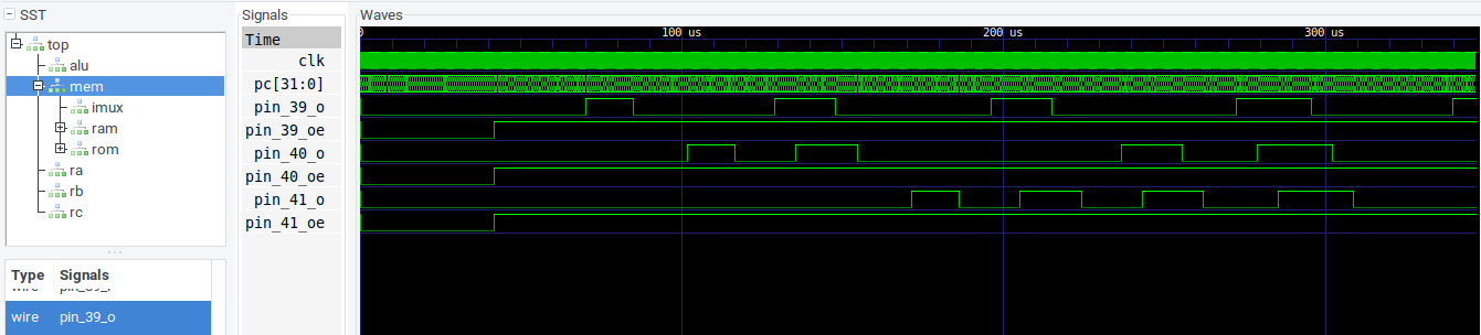
With the program modified to toggle the LEDs more quickly, you can see the transitions on the waveform viewer.
So far, so good. Now, we can build the design by adding a command-line option to call the build method from our modified board file. I decided to use the -b option for that, like in my last post about nMigen. So you can replace the __main__ method with:
from upduino import *

# 'main' method to run a basic testbench.
if __name__ == "__main__":
  if ( len( sys.argv ) == 2 ) and ( sys.argv[ 1 ] == '-b' ):
    # Build the application for an iCE40UP5K FPGA.
    # Currently, this is meaningless, because it builds the CPU
    # with a hard-coded 'infinite loop' ROM. But it's a start.
    with warnings.catch_warnings():
      warnings.filterwarnings( "ignore", category = DriverConflict )
      warnings.filterwarnings( "ignore", category = UnusedElaboratable )
      # Build the CPU to read its program from a 2MB offset in SPI Flash.
      prog_start = ( 2 * 1024 * 1024 )
      cpu = CPU( SPI_ROM( prog_start, prog_start * 2, None ) )
      UpduinoPlatform().build( ResetInserter( cpu.clk_rst )( cpu ),
                               do_program = False )
  else:
    # Run testbench simulations.
    with warnings.catch_warnings():
      warnings.filterwarnings( "ignore", category = DriverConflict )

      print( '--- CPU Tests ---' )
      # Simulate the 'infinite loop' ROM to screen for syntax errors.
      cpu_sim( loop_test )
      cpu_spi_sim( loop_test )
      cpu_sim( ram_pc_test )
      cpu_spi_sim( ram_pc_test )
      cpu_sim( add_test )
      cpu_sim( addi_test )
      cpu_sim( and_test )
      cpu_sim( andi_test )
      # (the rest of the compliance tests)

      # Done; print results.
      print( "CPU Tests: %d Passed, %d Failed"%( p, f ) )
Notice that the ResetInserter nMigen function is used to set up the CPU’s clk_rst signal as the default sync clock domain’s reset signal. When a clock domain’s reset signal gets toggled, all of the signals which are controlled by that domain will revert to their reset values. This is a good reason to set reset = x when you create new Signal objects; if you add something like a debugging peripheral or watchdog timer later on, you will have a quick and easy way to reset the whole design.
Now if you run python3 cpu.py -b, the design should build for an iCE40UP5K-SG48 chip like the one found on an Upduino board. The bitstream will be saved as build/top.bin, and you can find reports in build/top.rpt or build/top.tim.
It’s easiest to flash the test program by running make flash in tests/hw_tests/led_test, because like I mentioned last time, it might take a few tries to re-flash a program once the FPGA starts to actively read from the Flash chip. Then, run iceprog build/top.bin to program the CPU design, and the board’s LEDs should start flashing. Yay!

Exciting that it works, but these LEDs are blindingly bright when they’re driven as a simple ‘on / off’ GPIO pin.
PWM Test: Pulsing LED
You can write a test of the PWM peripheral with the same general approach as the GPIO test program. I made a new tests/hw_tests/pwm_test/ subdirectory, and copied the same Makefile from the GPIO test into it. The main.c file can also look similar:
// Standard library includes.
#include <stdint.h>
#include <string.h>
// Device header files
#include "encoding.h"
#include "cpu.h"

// Pre-defined memory locations for program initialization.
extern uint32_t _sidata, _sdata, _edata, _sbss, _ebss;
// 'main' method which gets called from the boot code.
int main( void ) {
  // Copy initialized data from .sidata (Flash) to .data (RAM)
  memcpy( &_sdata, &_sidata, ( ( void* )&_edata - ( void* )&_sdata ) );
  // Clear the .bss RAM section.
  memset( &_sbss, 0x00, ( ( void* )&_ebss - ( void* )&_sbss ) );

  // Connect pins 39-41 to PWM peripherals 1-3.
  IOMUX->CFG5 |= ( IOMUX_PWM1 << IOMUX39_O );
  IOMUX->CFG6 |= ( ( IOMUX_PWM2 << IOMUX40_O ) |
                   ( IOMUX_PWM3 << IOMUX41_O ) );
  // Increment a counter and set the PWM 'compare' values from it.
  int counter = 0;
  int gdir = 1;
  int bdir = -1;
  int rdir = 1;
  int g = 0;
  int b = 10;
  int r = 20;
  while( 1 ) {
    ++counter;
    // Don't increment color values on every tick, so the
    // color transitions are visible.
    if ( ( ( counter & 0xFF ) == 0 ) && ( counter & 0x100 ) ) {
      g += gdir;
      b += bdir;
      r += rdir;
      // Don't go all the way up to max brightness.
      if ( ( g == 0x1F ) || ( g == 0 ) ) { gdir = -gdir; }
      if ( ( b == 0x1F ) || ( b == 0 ) ) { bdir = -bdir; }
      if ( ( r == 0x1F ) || ( r == 0 ) ) { rdir = -rdir; }
      // Apply the new colors.
      PWM1->CR = g;
      PWM2->CR = b;
      PWM3->CR = r;
    }
  }
  return 0; // lol
}
It connects pins 39-41 to the three PWM peripherals, and then sets “compare” values in each peripheral to pulse each color. If you build and upload that program, the LEDs should start to dim and brighten through various colors.
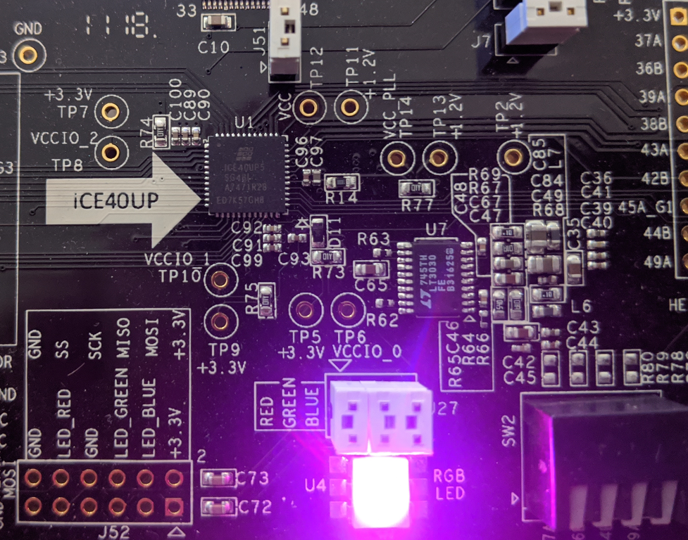
That’s better – PWM lets you make less “harsh” LED patterns by having colors fade and merge into each other.
Conclusions
Phew – congratulations on getting through all of that! I’m sure there are still some bugs, and I could probably use some hardware design pointers. And I’m sorry if I glossed over anything; it was a lot to cover in one article.
When I build this design with three PWM peripherals, it uses 68% of the FPGA’s LUT4s (3604 / 5280) and has a predicted maximum speed of 12.61MHz, which isn’t great. The SPI Flash access time is also laughably slow, since it takes so many clock cycles to load each word.
But as far as starting points go, it could be worse. It has room for a few more peripherals and it seems capable of running C code built with the RISC-V GNU toolchain, which is pretty neat. If you ran into trouble with any of the modules, don’t forget that there is a design implementing this code available on GitHub.
I’d also like to give a huge thanks to whitequrk, ZirconiumX, sorear, awygle, daveshah, Degi, MadHacker, adamgreig, and the rest of the friendly folks on the #nmigen and #riscv freenode IRC channels. This design would have turned out much worse without the benefit of their advice and patience.
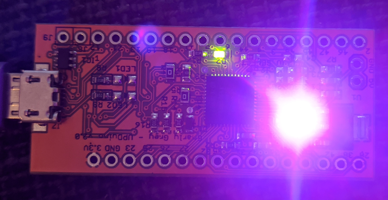

Luke Kenneth Casson Leighton
August 10, 2020 at 6:13 am
this is fantastic work, can i suggest talking to florent from enjoy-digital.fr to add it as a supported platform to litex? it was pure coincidence that i found this and it could be really useful in so many areas.
my only criticism is this: i cannot read the code and work out where imports are coming from, what the code structure is, which are the modules that you created and which are nmigen or anything else, and the reason is because you have followed the 20-year widely and strongly discouraged practice of using wildcard imports.
wildcard imports are strongly discouraged across the internet: you can find any number of articles that explain why they are harmful. however the one that is most damaging is not even listed in any of the posts explaining why it is bad practice, and it’s this: you are the only one who can easily read the code.
the only people who can help you debug this code without asking questions “where is this imported from, where is this imported from” is you – or those people who have fully memorised every single line of every single module that, by coincidence, they happen also to have used.
if this is not a problem for you – if you have no intention of collaborating with anyone – then that is perfectly fine. however be aware that this is the consequence of choosing this particular practice: collaboration is severely hampered.
Vivonomicon
August 15, 2020 at 10:04 am
Thank you for the feedback! You’re right, I should clean things up and use more specific import statements. I should also probably add things like `__all__` attributes to the local modules, but you know how it is…time makes fools of us all.
In this case, I was mostly trying to learn about nMigen and HDL design; I think that what I came up with is too large and slow for the standards of a commercial project. If I do come back to this project, readability is certainly one of the first things that I’d like to improve, but I might wait until there is a bit more documentation for nMigen’s usage and APIs.
Anyways, thanks again for the pointers.