
Like many of us, I’ve been stuck indoors without much to do for the past month or so. Unfortunately, I’m also in the process of moving, so I don’t know anyone in the local area and most of my ‘maker’ equipment is in storage. But there’s not much point in sulking for N months straight, so I’ve been looking at this as an opportunity to learn about designing and implementing FPGA circuits.
I tried getting into Verilog a little while ago, but that didn’t go too well. I did manage to write a simple WS2812B “NeoPixel” driver, but it was clunky and I got bored soon after. In my defense, Verilog and VHDL are not exactly user-friendly or easy to learn. They can do amazing things in the hands of people who know how to use them, but they also have a steep learning curve.
Luckily for us novices, open-source FPGA development tools have advanced in leaps and bounds over the past few years. The yosys and nextpnr projects have provided free and (mostly) vendor-agnostic tools to build designs for real hardware. And a handful of high-level code generators have also emerged to do the heavy lifting of generating Verilog or VHDL code from more user-friendly languages. Examples of those include the SpinalHDL Scala libraries, and the nMigen Python libraries which I’ll be talking about in this post.
I’ve been using nMigen to write a simple RISC-V microcontroller over the past couple of months, mostly as a learning exercise. But I also like the idea of using an open-source MCU for smaller projects where I would currently use something like an STM32 or MSP430. And most importantly, I really want some dedicated peripherals for driving cheap addressable “NeoPixel” LEDs; I’m tired of needing to mis-use a SPI peripheral or write carefully-timed assembly code which cannot run while interrupts are active.
But that will have to wait for a follow-up post; for now, I’m going to talk about some simpler tasks to introduce nMigen. In this post, we will learn how to read “program data” from the SPI Flash chip on an iCE40 FPGA board, and how to use that data to light up the on-board LEDs in programmable patterns.
The LEDs on these boards are very bright, because you’re supposed to use PWM to drive them.
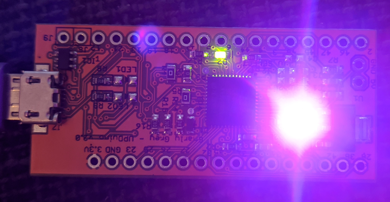
The target hardware will be an iCE40UP5K-SG48 chip, but nMigen is cross-platform so it should be easy to adapt this code for other FPGAs. If you want to follow along, you can find a 48-pin iCE40UP5K on an $8-20 “Upduino” board or a $50 Lattice evaluation board. If you get an “Upduino”, be careful not to mis-configure the SPI Flash pins; theoretically, you could effectively brick the board if you made it impossible to communicate with the Flash chip. The Lattice evaluation board has jumpers which you could unplug to recover if that happens, but I don’t think that the code presented here should cause those sorts of problems. I haven’t managed to brick anything yet, knock on wood…
Be aware that the Upduino v1 board is cheaper because it does not include the FT2232 USB/SPI chip which the toolchain expects to communicate with, so if you decide to use that option, you’ll need to know how to manually write a binary file to SPI Flash in lieu of the iceprog commands listed later in this post.
Toolchain Setup
nMigen appears to be the continuation of a project called Migen, which is already used in a number of cool projects such as the “LiteX” System-on-Chip generator. It is still under very active development, so the syntax presented in this post may go out of date eventually, but it seems stable enough to use with quite complex designs. It also includes a built-in simulator which is very easy to use, so you can verify your designs before trying them in hardware without much extra effort.
A wide variety of FPGA toolchains are supported, including closed-source ones. It outputs designs in an intermediate representation which yosys can convert to Verilog, so if you want to use nMigen with a big expensive Xilinx chip, you can! I opted to use a Lattice iCE40UP5K chip for learning, though, because it is cheap and available in a hobbyist-friendly QFN package. It also has more resources than the iCE40HX1K found on the popular “Icestick” board, with 5,280 LUTs and (I think) 128KB of on-chip RAM.
So if you want to follow along, you’ll need to install the yosys, nextpnr-ice40, and icestorm toolchains:
- https://github.com/YosysHQ/yosys
- https://github.com/YosysHQ/nextpnr
- https://github.com/cliffordwolf/icestorm
Each of those repositories contains its own list of prerequisites and build instructions, which seem pretty straightforward for basic installations. The nMigen libraries are distributed as Python 3.x packages, so you can install them through the pip3 package manager or by copying each package into your library installation path:
- https://github.com/nmigen/nmigen/
- https://github.com/nmigen/nmigen-boards
- https://github.com/nmigen/nmigen-soc/
I just copied the packages into ~/.local/lib/python3.6/site-packages/, but if you use Python a lot, you might already have a preferred way to install new libraries. Either way, be sure to copy the package directories (nmigen-boards/nmigen_boards/, etc), not the entire repository (nmigen-boards/, etc).
The nmigen-boards repository contains descriptions of the hardware resources on different FPGA development boards, and the nmigen-soc repository contains extra building blocks for creating System-on-Chip designs, including a Wishbone bus implementation. The nmigen repository contains the core project, as you might expect.
Finally, you’ll probably want a way to view the simulated results of the tests which you’ll write for your design – you are going to write tests, right? Those “waveform” results will be saved as .vcd “Value Change Dump” files, and if you don’t have a preferred way to open those files, gtkwave is a free option which is pretty easy to get started with.
Getting Started with nMigen
A brief word about digital circuits before we start: in general, FPGA designs use two basic types of logic: “synchronous” logic which perform reads/writes when a clock signal rises or falls, and “combinatorial” logic which reads/writes as quickly as the signals can move through the tiny gates and wires inside the chip. Synchronous logic uses flip-flops to “latch” an input value at each clock edge, which guarantees that the output value will only change at the start or end of each clock cycle. Combinatorial logic allows the output value to change at any time, which lets signals travel as quickly as the charge carriers can propagate through the circuit. But different circuit elements usually take different lengths of time to complete, so the output of a combinatorial circuit will usually experience ‘glitches’ before it eventually settles on the correct value. It follows that your synchronous logic’s top speed will generally be limited by the longest route (“critical path”) through your combinatorial logic.
I hope that explains enough for a newcomer to understand the simple designs that we’re about to go over, but if you are interested in the subject and not entirely satisfied by that very brief explanation, check out the free “computation structures” online course, which is based off of MIT’s sadly discontinued 6.004.x edX classes.
Writing a Simple Circuit
Before we write logic to communicate with external devices like SPI Flash, let’s get familiar with nMigen by writing and simulating a simple “Hello, World” design which increments a counter using synchronous logic.
nMigen designs are structured as a tree of nested “modules”: you create a “parent” module, and add “child” modules (which can each have their own set of “child” modules) to it. When you want to test or run your design, you simulate or build the top-level “parent” module. Each module is structured as a Python class, with an __init__ method to initialize its resources and an elaborate method to describe its runtime logic.
You can create different types of synchronous logic with nMigen, but by default, there is one sync “clock domain” which acts on the rising edge of the default clock, and one comb domain for combinatorial logic. With that in mind, take a look at this minimal nMigen module, which you can put in an ordinary .py file:
from nmigen import *

class TestModule( Elaboratable ):
  def __init__( self ):
    self.count = Signal( 16, reset = 0 )
    self.ncount = Signal( 16, reset = 0 )

  def elaborate( self, platform ):
    m = Module()
    m.d.comb += self.ncount.eq( ~self.count )
    m.d.sync += self.count.eq( self.count + 1 )
    return m
This design will increment a 16-bit counter at each rising clock edge, and its combinatorial logic will try to ensure that another 16-bit value is always the bitwise opposite of the counter. Notice that the module inherits from Elaboratable and implements the abstract elaborate( self, platform ) method which returns a Module object describing its runtime logic. The platform variable contains information about the hardware which the design is being built for, and it is set to None when the design is built to run in a simulator.
The sync and comb logic domains are accessed through the Module’s d (“domain”) attribute, and you can add “rules” to them with the += operator. x.eq( y ) is a simple rule which translates to x = y. If a module’s state ends up with more than one rule targeting the same signal, the rule which comes “later” in the design will take precedence. So if we wanted to reset the count signal to zero when it reaches a value of 42, we could override the count = count + 1 logic like this:
  def elaborate( self, platform ):
    m = Module()
    m.d.comb += self.ncount.eq( ~self.count )
    m.d.sync += self.count.eq( self.count + 1 )
    with m.If( self.count == 42 ):
      m.d.sync += self.count.eq( 0 )
    return m
Notice that the conditional statement uses m.If(...): instead of if ...:. We’re describing behavior which can change as the FPGA design runs, so we defer to the Module object to evaluate the condition. You should only use Python if/elif/else statements for conditions which will never change, such as configuration flags which determine whether features will be included in the design.
You can also only write to each signal from one domain, so this code would not work:
def elaborate( self, platform ):
  m = Module()
  m.d.comb += self.ncount.eq( ~self.count )
  m.d.sync += self.count.eq( self.count + 1 )
  with m.If( self.count == 42 ):
    m.d.comb += self.count.eq( 0 )
  return m
Since it tries to write to count from both the sync and comb domains at different points in the design, you’ll see an error like this if you try to simulate or build it:
nmigen.hdl.dsl.SyntaxError: Driver-driver conflict: trying to drive (sig count) from d.comb, but it is already driven from d.sync
Simulating and Testing a Design
Now, if you were to run the previous error-free design, it seems pretty clear that the count value should equal 3 after 3 clock cycles. But it’s always a good idea to double-check your assumptions by simulating a design before you build and run it on an FPGA. Fortunately, nMigen makes it very easy to simulate a design; you can add something like this to the end of your module’s .py file:
from nmigen.back.pysim import *

if __name__ == "__main__":
  dut = TestModule()
  with Simulator( dut, vcd_file = open( 'test.vcd', 'w' ) ) as sim:
    def proc():
      for i in range( 50 ):
        yield Tick()
    sim.add_clock( 1e-6 )
    sim.add_sync_process( proc )
    sim.run()
The if __name__ == "__main__": line is Python-ese for “only run this logic if the file is being executed”, and dut is a common variable name which means “Device Under Test”.
The above logic sets up a simulation to output its results to a file called test.vcd. The add_clock method adds a clock signal which ticks once every 0.000001 seconds, and which will drive the default sync clock domain. Then the proc test process is added to the simulation and run; in this case, it simply waits 50 clock ticks before finishing.
If you run the resulting file with python3 test.py, the simulation will run. It won’t print anything out, but it will create a test.vcd file which you can open and view with a program like gtkwave:
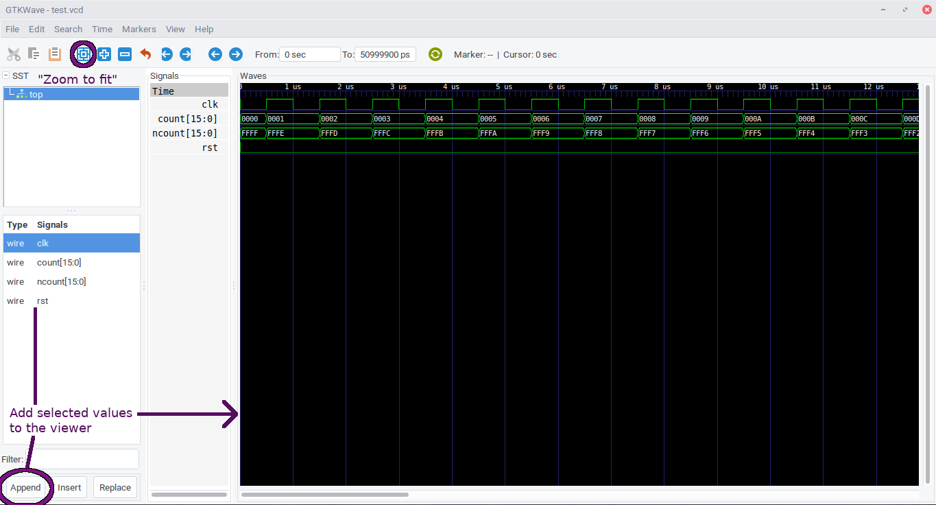
gtkwave rendering of the minimal test design
You can also write unit tests by reading values out of the simulation using yield. And if you write any helper functions to run within the simulation, they should be called with yield from func(...). For example, this test process would check that the count value always equals the number of ticks which have elapsed since the simulation started:
    def proc():
      for i in range( 50 ):
        c = yield dut.count
        if c == i:
          print( "PASS: count == %d"%i )
        else:
          print( "FAIL: count != %d (got: %d)"%( i, c ) )
        yield Tick()
If you run that, you should see failures starting at tick 42 because our design resets the counter at that point:
PASS: count == 0
PASS: count == 1
PASS: count == 2
PASS: count == 3
[...]
PASS: count == 41
PASS: count == 42
FAIL: count != 43 (got: 0)
FAIL: count != 44 (got: 1)
FAIL: count != 45 (got: 2)
[...]
If you want to check combinatorial values in a simulation, you should also call yield Settle() before checking the value, to let the combinatorial signals settle on their correct value.
You can find this example code on GitHub, if you don’t want to copy/paste.
Blinking an LED
Now that we know how to increment a value, let’s toggle an LED on an interval. To do that, we’ll need to access our FPGA board’s I/O pins. These are defined in “board files”, which you can find in the nmigen-boards repository. The “Upduino” and Lattice evaluation boards both include a common-cathode RGB LED on the same 3 pins, and nMigen lets you access hardware resources by name and index, so we can use the same design to target both boards. In fact, since we’re only going to use the LED and SPI Flash resources, you can build the design for an Upduino board and run it on a Lattice evaluation board, and vice-versa.
The LED resources are aliased to led_r, led_g, and led_b. Once you request a pin resource from the platform object, you can access its input and output values with pin.i and pin.o. LEDs are output-only, so the following code will set the green LED to the 20th bit of the count value, and the blue LED to the opposite of that:
class TestLEDModule( Elaboratable ):
  def __init__( self ):
    self.count = Signal( 32, reset = 0 )

  def elaborate( self, platform ):
    m = Module()

    m.d.sync += self.count.eq( self.count + 1 )
    if platform is not None:
      grn_led = platform.request( 'led_g', 0 )
      blu_led = platform.request( 'led_b', 0 )
      m.d.comb += [
        grn_led.o.eq( self.count[ 20 ] ),
        blu_led.o.eq( ~grn_led.o )
      ]

    return m
It’s a good idea to put platform resource logic under an if platform is not None: check, so that they do not cause errors when you simulate the design. Remember, the platform value is only provided when you are building a design for actual hardware. To build a design, you can simply use the build method provided by the board file. For an “Upduino v2” board, you can append this to the end of the file:
from nmigen_boards.upduino_v2 import *

if __name__ == "__main__":
  dut = TestLEDModule()
  UpduinoV2Platform().build( dut )
It’s usually a good idea to include a way to choose between simulating and building a design, but we’ll do that in the next example. For the sake of brevity, you can just run your led.py file to build this example. The results will be placed in a build/ directory. The top.rpt file is a report which tells you how much of the FPGA’s resources are used in the design, and the top.tim file is a timing analysis which tells you how quickly its synchronous logic will probably be able to run.
The top.bin file contains the actual FPGA configuration bitstream, and you can upload that to your board with the iceprog utility:
iceprog build/top.bin
Once that command completes, the board’s LED should start blinking between a blue and green color. Hooray. And again, you can find this example project on GitHub.
Reading from Memory
Almost every iCE40 development board includes an external SPI Flash chip to store their configurations. This type of FPGA does have non-volatile memory inside of the chip, but you can only ever write to it once and it’s supposed to have a separate 2.5V power supply to run properly. So for multi-use development, iCE40s also include hardware to read their configuration out of a commodity SPI Flash chip, such as a Winbond W25Q series or similar.
These chips are usually sized to at least 2x the expected maximum size of the FPGA’s configuration bitstream, so you can use the leftover space to store “program data”, similar to the Flash memory on a microcontroller. Memory access will be comparatively slow, since you’ll need to wait several dozen clock cycles every time that you want to read a word of data, but this is just an example.
To test reading data from the Flash chip, we can write a new module which contains a simple state machine to read data, and a parent module which acts like a very simple CPU. The parent module will increment the address that it reads from, and depending on the returned value, it will either delay for a given number of cycles, toggle one of the LEDs, or jump back to address zero. This will let us write simple “programs” which set the LEDs to different colors at different times.
Simulating Memory on a Wishbone Bus
Before writing the actual SPI Flash module, let’s write and test the parent “CPU” module with simulated memory values. The SPI interface has a few “gotchas” and places where incorrect timing can cause problems, so it’s a good idea to make sure that the basic program logic works before diving into that.
The parent “CPU” module needs to be able to request new reads and wait for the child memory module to finish, without knowing how long a memory access will take ahead of time. This is a common problem which people have already developed standards for, so I’m going to use the free Wishbone Bus standard to mediate data transfers. nMigen includes an implementation of this sort of bus in the nmigen-soc repository, so it is nice and easy to use in a design. We can make our memory module inherit from nmigen_soc.wishbone.Interface, call the parent __init__ method with the desired address and data widths during initialization, and then access the bus signals with self.<signal>.
I’m still learning about the Wishbone bus, so these descriptions may not be completely accurate, but as I understand it, these are the relevant signals for a simple read-only memory:
ack: “acknowledge” signal which is asserted by the child when it is finished with a transaction.cyc: “cycle” signal which is asserted by the parent when a bus transaction is ongoing. The child should ignore any inputs and avoid asserting any outputs when “cycle” is not asserted.stb: “strobe” signal which is asserted by the parent when a bus transfer cycle is ongoing. The “strobe” signal can be toggled multiple times while the “cycle” signal is asserted to perform multiple transfers in a single transaction.dat_r: “read data” buffer which the child fills with data to be read by the parent onceackis asserted.
The Wishbone specification uses “master” and “slave” if you’re following along in the documentation; I prefer terminology like “parent” / “child” or “host” / “device”, but I realize that can cause some confusion and I’m sorry about that. Anyways, you can set up a simple word-addressed read-only Wishbone memory like this:
from nmigen import *
from math import ceil, log2
from nmigen_soc.memory import *
from nmigen_soc.wishbone import *

# Simulated read-only memory module.
class ROM( Elaboratable, Interface ):
  def __init__( self, data ):
    # Record size.
    self.size = len( data )
    # Data storage.
    self.data = Memory( width = 32, depth = self.size, init = data )
    # Memory read port.
    self.r = self.data.read_port()

    # Initialize Wishbone bus interface.
    Interface.__init__( self,
                        data_width = 32,
                        addr_width = ceil( log2( self.size + 1 ) ) )
    self.memory_map = MemoryMap( data_width = self.data_width,
                                 addr_width = self.addr_width,
                                 alignment = 0 )

  def elaborate( self, platform ):
    m = Module()
    # Register the read port submodule.
    m.submodules.r = self.r

    # 'ack' signal should rest at 0.
    m.d.sync += self.ack.eq( 0 )
    # Simulated reads only take one cycle, but only acknowledge
    # them after 'cyc' and 'stb' are asserted.
    with m.If( self.cyc ):
      m.d.sync += self.ack.eq( self.stb )

    # Set 'dat_r' bus signal to the value in the
    # requested 'data' array index.
    m.d.comb += [
      self.r.addr.eq( self.adr ),
      self.dat_r.eq( self.r.data )
    ]

    # End of simulated memory module.
    return m
The MemoryMap object lets you describe the structure of different registers and memory spaces within an Interface. That isn’t necessary in a simple implementation like this, but nMigen will produce an error if you don’t assign one, so I initialized an empty one with the same address/data width as the bus and no alignment restrictions.
The Memory class is an efficient way to store data in the FPGA; I think it asks the synthesizer to try to use storage resources like RAM instead of the scarcer and more precious LUTs / flip-flops / etc. When you are simulating a design, you can access Memory data using array syntax (e.g. data[ 0 ]), but you need to use read and write ports when you build a design for real hardware. Read ports are pretty easy to use: set port.addr, wait a cycle, read port.data. Write ports are similar, but they also have an en “enable” attribute which prevents writes when it is de-asserted.
And since you should always simulate your modules before running them (ignore the above LED example), here’s an example testbench:
from nmigen.back.pysim import *

# Testbench:
# Perform an individual 'memory read' unit test.
def rom_read_ut( rom, address, expected ):
  # Set address, and wait a tick.
  yield rom.adr.eq( address )
  yield Tick()
  # Done. Check the result after combinatorial logic settles.
  yield Settle()
  actual = yield rom.dat_r
  if expected == actual:
    print( "PASS: Memory[ 0x%04X ] = 0x%08X"%( address, expected ) )
  else:
    print( "FAIL: Memory[ 0x%04X ] = 0x%08X (got: 0x%08X)"
           %( address, expected, actual ) )

# Run a basic series of tests when this file is run.
if __name__ == "__main__":
  # Create a test memory with 20 bytes of data.
  dut = ROM( [ 0x01234567, 0x89ABCDEF,
               0x0C0FFEE0, 0xDEC0FFEE,
               0xFEEBEEDE ] )
  # Run the simulation.
  with Simulator( dut, vcd_file = open( 'rom.vcd', 'w' ) ) as sim:
    def proc():
      # Test reads.
      yield from rom_read_ut( dut, 0, 0x01234567 )
      yield from rom_read_ut( dut, 1, 0x89ABCDEF )
      yield from rom_read_ut( dut, 2, 0x0C0FFEE0 )
      yield from rom_read_ut( dut, 3, 0xDEC0FFEE )
      yield from rom_read_ut( dut, 4, 0xFEEBEEDE )
    sim.add_clock( 1e-6 )
    sim.add_sync_process( proc )
    sim.run()
Try running the full rom.py file (which you can also find on GitHub), and inspect the signals in the rom.vcd file. Notice how the read data follows the address by one clock cycle; it would be nice to be able to perform single-cycle access, but I am learning that FPGA design is full of tradeoffs between speed and size.
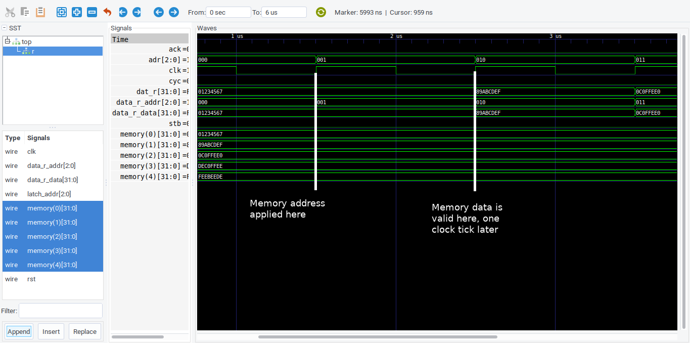
Memory access through a ‘read port’ is delayed by one clock cycle.
Writing a Simple State Machine
Now that we have a simulated memory module, we can write the parent “CPU” state machine in a separate top.py file. (It looks like “top” is often used as a default name for top-level parent modules.) First, let’s define a simple set of usable commands to toggle each LED, delay for a variable number of cycles, and return to address 0:
# Basic instruction definitions.
# Red LED on/off
RED_ON  = 0x00000009
RED_OFF = 0x00000001
# Green LED on/off
GRN_ON  = 0x0000000A
GRN_OFF = 0x00000002
# Blue LED on/off
BLU_ON  = 0x0000000B
BLU_OFF = 0x00000003
# Delay for a number of cycles.
def DELAY( cycles ):
  return ( ( 0x4 | ( cycles << 4 ) ) & 0xFFFFFFFF )
# Jump back to word 0.
RETURN  = 0x00000000
It’s also a good idea to define a ‘dummy LED’ class to use when simulating the design; it will let you avoid unnecessary if statements around the LED logic, and it will let you see the LED signals in the simulation results. You can use the ‘name’ keyword argument to set a signal’s name in the simulation output, otherwise it will use the name of the variable followed by $<number> if the name is re-used:
# Dummy LED class for testing.
class DummyLED():
  def __init__( self, name ):
    self.o = Signal( 1, reset = 0b0, name = '%s_o'%name )
Next, we can write some basic initialization logic to define the signals which the state machine will need to keep track of:
class Memory_Test( Elaboratable ):
  def __init__( self, memory ):
    # Simulated memory module.
    self.mem = memory
    # Current memory pointer.
    self.pc = Signal( self.mem.addr_width, reset = 0 )
    # Delay counter.
    self.dc = Signal( 28, reset = 0 )
Finally, we can define the state machine itself with the elaborate method. nMigen has some special syntax for evaluating a simple Finite State Machine. You start with a with m.FSM(): statement, then you define each state using with m.State( "this_state" ): block. And to move to another state at the next clock tick, you can set m.next = "next_state". So you can implement a simple “read, execute, increment address” state machine like this:
def elaborate( self, platform ):
  m = Module()
  m.submodules.mem = self.mem

  # LED resources.
  if platform is None:
    rled = DummyLED( 'led_r' )
    gled = DummyLED( 'led_g' )
    bled = DummyLED( 'led_b' )
  else:
    rled = platform.request( 'led_r', 0 )
    gled = platform.request( 'led_g', 0 )
    bled = platform.request( 'led_b', 0 )

  # Set bus address to the 'program counter' value.
  m.d.comb += self.mem.adr.eq( self.pc )

  # State machine:
  # * 'FETCH':   Retrieve the next instruction from memory.
  # * 'PROCESS': Execute the current instruction.
  with m.FSM():
    # 'FETCH' state: Get the next word from memory.
    with m.State( 'FETCH' ):
      # Pulse 'stb' and 'cyc' to start the bus transaction.
      m.d.sync += [
        self.mem.stb.eq( 1 ),
        self.mem.cyc.eq( 1 )
      ]
      # Proceed once 'ack' is asserted.
      with m.If( self.mem.ack == 1 ):
        # Reset the delay counter, and clear 'stb' / 'cyc' to end
        # the bus transaction. This also causes 'ack' to be cleared.
        m.d.sync += [
          self.dc.eq( 0 ),
          self.mem.stb.eq( 0 ),
          self.mem.cyc.eq( 0 )
        ]
        m.next = 'PROCESS'
      # Read is ongoing while 'ack' is not asserted.
      with m.Else():
        m.next = 'FETCH'
    # 'PROCESS' state: execute the retrieved instruction.
    with m.State( 'PROCESS' ):
      # Unless otherwise specified, increment the PC address
      # and proceed back to the 'FETCH' state.
      m.d.sync += self.pc.eq( self.pc + 1 )
      m.next = 'FETCH'
      # If the word is 0 or -1, reset PC address to 0 instead of
      # incrementing it. 0xFFFFFFFF can indicate an error or
      # uninitialized SPI memory, so it's a good 'return' trigger.
      with m.If( ( self.mem.dat_r == 0x00000000 ) |
                 ( self.mem.dat_r == 0xFFFFFFFF ) ):
        m.d.sync += self.pc.eq( 0 )
      # If the 4 LSbits equal 0x4, delay for a number of cycles
      # indicated by the remaining 28 MSbits.
      with m.Elif( self.mem.dat_r[ :4 ] == 4 ):
        # If the delay has not finished, increment 'delay counter'
        # without changing the PC address, and return to the
        # 'PROCESS' state instead of moving on to 'NEXT'.
        with m.If( self.dc != ( self.mem.dat_r >> 4 ) ):
          m.d.sync += [
            self.dc.eq( self.dc + 1 ),
            self.pc.eq( self.pc )
          ]
          m.next = 'PROCESS'
      # If the 3 LSbits == 3, set the blue LED to the 4th bit.
      with m.Elif( self.mem.dat_r[ :3 ] == 3 ):
        m.d.sync += bled.o.eq( self.mem.dat_r[ 3 ] )
      # If the 3 LSbits == 2, set the green LED to the 4th bit.
      with m.Elif( self.mem.dat_r[ :3 ] == 2 ):
        m.d.sync += gled.o.eq( self.mem.dat_r[ 3 ] )
      # If the 3 LSbits == 1, set the red LED to the 4th bit.
      with m.Elif( self.mem.dat_r[ :3 ] == 1 ):
        m.d.sync += rled.o.eq( self.mem.dat_r[ 3 ] )

  # (End of memory and finite state machine test logic.)
  return m
I made the ‘return to address 0’ instruction accept either 0x00000000 or 0xFFFFFFFF, because the default state of SPI Flash memory is a 1, not a 0. There are also usually pull-up resistors on the data lines, so if you end up reading from an area of memory that has never been written to or failing to read data entirely, you’ll probably receive a value of 0xFFFFFFFF. And it would be nice to avoid side effects when…uh, I mean “if”… that happens.
Next, you can define a ROM simulated memory module with an array containing a series of instructions, and simulate it for a few hundred cycles:
if __name__ == "__main__":
  dut = Memory_Test( ROM( [
    BLU_ON, DELAY( 5 ), GRN_ON, DELAY( 5 ), BLU_OFF, RED_ON,
    DELAY( 10 ), RED_OFF, DELAY( 5 ), GRN_OFF, DELAY( 5 ), RETURN
  ] ) )
  with Simulator( dut, vcd_file = open( 'test.vcd', 'w' ) ) as sim:
    # Simulate running for 200 clock cycles.
    def proc():
      for i in range( 200 ):
        yield Tick()
        yield Settle()
    sim.add_clock( 1e-6 )
    sim.add_sync_process( proc )
    sim.run()
If you open the resulting test.vcd file, you should see the LEDs turning on and off in time with the program image:
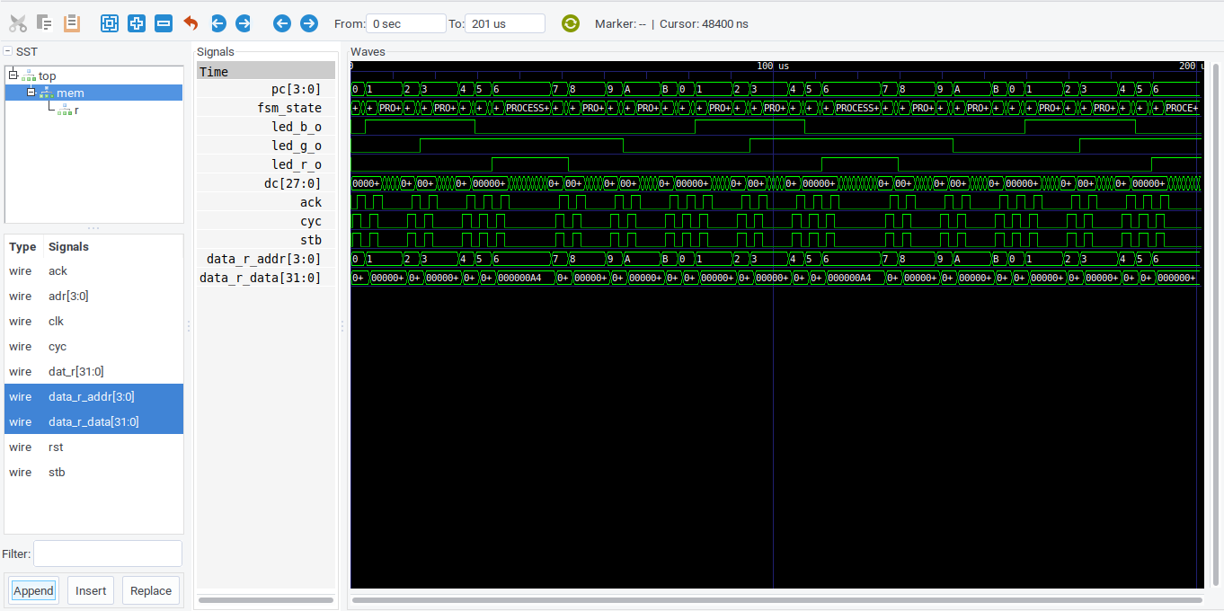
viewing the results of running the Finite State Machine test design. Notice that the LED signals toggle in time with the instructions listed above.
With the simulation looking good, you can add an option to build the design instead of simulating it. There are probably better ways to process command-line arguments in Python, but one easy option is to use sys.argv:
from nmigen_boards.upduino_v2 import *

# 'main' method to simulate or build the test.
if __name__ == "__main__":
  # If the file was run with '-b', build for an 'Upduino' board
  if ( len( sys.argv ) == 2 ) and ( sys.argv[ 1 ] == '-b' ):
    dut = Memory_Test( ROM( [
      BLU_ON, DELAY( 500000 ), GRN_ON, DELAY( 500000 ),
      BLU_OFF, RED_ON, DELAY( 1000000 ), RED_OFF,
      DELAY( 500000 ), GRN_OFF, DELAY( 500000 ), RETURN
    ] ) )
    UpduinoV2Platform().build( dut )
  # If no arguments were passed in, simulate the design.
  else:
    dut = Memory_Test( ROM( [
      BLU_ON, DELAY( 5 ), GRN_ON, DELAY( 5 ), BLU_OFF, RED_ON,
      DELAY( 10 ), RED_OFF, DELAY( 5 ), GRN_OFF, DELAY( 5 ), RETURN
    ] ) )
    with Simulator( dut, vcd_file = open( 'test.vcd', 'w' ) ) as sim:
      # Simulate running for 200 clock cycles.
      def proc():
        for i in range( 200 ):
          yield Tick()
          yield Settle()
      sim.add_clock( 1e-6 )
      sim.add_sync_process( proc )
      sim.run()
With that, you should be able to build the design with python3 top.py -b, and program it with iceprog build/top.bin. The LEDs on the board should flash with the timing of your program, but notice how large the ‘delay’ values are in the test program above. It’s easier to look at transitions when you use small delay values, but if you do that with a fast clock rate, the LED might look white as the colors blur together.
Reading from SPI Flash
Now that you have a basic state machine which can run a few different instructions, it’s time to read a program out of the board’s SPI Flash chip. Since we implemented the simulated memory module as a standard Wishbone bus, we can write a SPI Flash module which implements the same Interface superclass and drop it in to the Memory_Test module with hardly any changes. The read-only SPI Flash memory module will have a slightly more complicated state machine, but it’s not too bad:
- 1. Wake up the Flash chip from sleep mode.
- 2. Wait for a read request from the parent module.
- 3. Send the 32-bit “read data from address X” command.
- 4. Receive 32 bits of data from the chip in little-endian order.
- 5. Assert a ‘done’ signal for the parent module to see, and go back to step 2.
It’s easy to accidentally use the wrong clock edge, but you can catch those sorts of mistakes by looking carefully at simulation results and the datasheet of whatever device you’re trying to talk to. The “wake up from sleep mode” command is also easy to miss, because it usually isn’t required when communicating with SPI Flash. But to save power and prevent unwanted writes, iCE40 chips issue a “go to sleep” command after they finish reading their configuration data.
So this isn’t the most efficient way to do it, but here’s a basic implementation of the state machine described above. Remember, you can find these files on GitHub if you don’t want to copy/paste everything:
from nmigen import *
from math import ceil, log2
from nmigen.back.pysim import *
from nmigen_soc.memory import *
from nmigen_soc.wishbone import *
from nmigen_boards.resources import *

# (Dummy SPI resources for simulated tests)
class DummyPin():
  def __init__( self, name ):
    self.o = Signal( name = '%s_o'%name )
    self.i = Signal( name = '%s_i'%name )
class DummySPI():
  def __init__( self ):
    self.cs   = DummyPin( 'cs' )
    self.clk  = DummyPin( 'clk' )
    self.mosi = DummyPin( 'mosi' )
    self.miso = DummyPin( 'miso' )

# Core SPI Flash "ROM" module.
class SPI_ROM( Elaboratable, Interface ):
  def __init__( self, dat_start, dat_end, data ):
    # Starting address in the Flash chip. This probably won't
    # be zero, because many FPGA boards use their external SPI
    # Flash to store the bitstream which configures the chip.
    self.dstart = dat_start
    # Last accessible address in the flash chip.
    self.dend = dat_end
    # Length of accessible data.
    self.dlen = ( dat_end - dat_start ) + 1
    # SPI Flash address command.
    self.spio = Signal( 32, reset = 0x03000000 )
    # Data counter.
    self.dc = Signal( 5, reset = 0b000000 )

    # Initialize Wishbone bus interface.
    Interface.__init__( self, addr_width = ceil( log2( self.dlen + 1 ) ), data_width = 32 )
    self.memory_map = MemoryMap( addr_width = self.addr_width, data_width = self.data_width, alignment = 0 )

    # Backing data store for a test ROM image. Not used when
    # the module is built for real hardware.
    if data is not None:
      self.data = Memory( width = 32, depth = len( data ), init = data )
    else:
      self.data = None

  def elaborate( self, platform ):
    m = Module()

    if platform is None:
      self.spi = DummySPI()
    else:
      self.spi = platform.request( 'spi_flash_1x' )

    # Clock rests at 0.
    m.d.comb += self.spi.clk.o.eq( 0 )
    # SPI Flash can only address 24 bits.
    m.d.comb += self.spio.eq( ( 0x03000000 | ( ( self.adr + self.dstart ) & 0x00FFFFFF ) ) )

    # Use a state machine for Flash access.
    # "Mode 0" SPI is very simple:
    # - Device is active when CS is low, inactive otherwise.
    # - Clock goes low, both sides write their bit if necessary.
    # - Clock goes high, both sides read their bit if necessary.
    # - Repeat ad nauseum.
    with m.FSM() as fsm:
      # 'Reset' and 'power-up' states:
      # pull CS low, then release power-down mode by sending 0xAB.
      # Normally this is not necessary, but iCE40 chips shut down
      # their connected SPI Flash after configuring themselves
      # in order to save power and prevent unintended writes.
      with m.State( "SPI_RESET" ):
        m.d.sync += self.spi.cs.o.eq( 1 )
        m.next = "SPI_POWERUP"
      with m.State( "SPI_POWERUP" ):
        m.d.sync += self.dc.eq( self.dc + 1 )
        m.d.comb += self.spi.clk.o.eq( ~ClockSignal( "sync" ) )
        m.d.comb += self.spi.mosi.o.eq( 0xAB >> ( 7 - self.dc ) )
        # Wait a few extra cycles after ending the transaction to
        # allow the chip to wake up from sleep mode.
        # TODO: Time this based on clock frequency?
        with m.If( self.dc == 30 ):
          m.d.sync += self.spi.cs.o.eq( 0 )
          m.next = "SPI_WAITING"
        # De-assert CS after sending 8 bits of data = 16 clock edges.
        with m.Elif( self.dc >= 8 ):
          m.d.sync += self.spi.cs.o.eq( 0 )
          m.next = "SPI_POWERUP"
        # Toggle the 'clk' pin every cycle.
        with m.Else():
          m.next = "SPI_POWERUP"
      # 'Waiting' state: Keep the 'cs' pin high until a new read is
      # requested, then move to 'SPI_TX' to send the read command.
      # Also keep 'ack' asserted until 'stb' is released.
      with m.State( "SPI_WAITING" ):
        m.d.sync += [
          self.ack.eq( self.cyc & ( self.ack & self.stb ) ),
          self.spi.cs.o.eq( 0 )
        ]
        m.next = "SPI_WAITING"
        with m.If( ( self.cyc == 1 ) & ( self.stb == 1 ) & ( self.ack == 0 ) ):
          m.d.sync += [
            self.spi.cs.o.eq( 1 ),
            self.ack.eq( 0 ),
            self.dc.eq( 31 )
          ]
          m.next = "SPI_TX"
      # 'Send read command' state: transmits the 0x03 'read' command
      # followed by the desired 24-bit address. (Encoded in 'spio')
      with m.State( "SPI_TX" ):
        # Set the 'mosi' pin to the next value and increment 'dc'.
        m.d.comb += self.spi.mosi.o.eq( self.spio >> self.dc )
        m.d.sync += self.dc.eq( self.dc - 1 )
        m.d.comb += self.spi.clk.o.eq( ~ClockSignal( "sync" ) )
        # Move to 'receive data' state once 32 bits have elapsed.
        # Also clear 'dat_r' and 'dc' before doing so.
        with m.If( self.dc == 0 ):
          m.d.sync += [
            self.dc.eq( 7 ),
            self.dat_r.eq( 0 )
          ]
          m.next = "SPI_RX"
        with m.Else():
          m.next = "SPI_TX"
      # 'Receive data' state: continue the clock signal and read
      # the 'miso' pin on rising edges.
      # You can keep the clock signal going to receive as many bytes
      # as you want, but this implementation only fetches one word.
      # Bytes are received in 'little-endian' format, MSbit-first.
      with m.State( "SPI_RX" ):
        # Simulate the 'miso' pin value for tests.
        if platform is None:
          m.d.comb += self.spi.miso.i.eq( ( self.data[ self.adr >> 2 ] >> self.dc ) & 0b1 )
        m.d.sync += [
          self.dc.eq( self.dc - 1 ),
          self.dat_r.eq( self.dat_r | ( self.spi.miso.i << self.dc ) )
        ]
        m.d.comb += self.spi.clk.o.eq( ~ClockSignal( "sync" ) )
        # Assert 'ack' signal and move back to 'waiting' state
        # once a whole word of data has been received.
        with m.If( self.dc[ :3 ] == 0 ):
          with m.If( self.dc[ 3 : 5 ] == 0b11 ):
            m.d.sync += [
              self.spi.cs.o.eq( 0 ),
              self.ack.eq( self.cyc )
            ]
            m.next = "SPI_WAITING"
          with m.Else():
            m.d.sync += self.dc.eq( self.dc + 15 )
            m.next = "SPI_RX"
        with m.Else():
          m.next = "SPI_RX"

    # (End of SPI Flash "ROM" module logic)
    return m
The SPI_RX state’s countdown value starts at 7 instead of 31 and occasionally increments by 15 instead of decrementing by 1. This is because the data will be returned from SPI Flash one byte at a time in “little-endian” order, with the lowest-address byte occupying the most-significant bits. This is how many processors organize data internally, but we human beings usually read and write hexadecimal values in “big-endian” order. It is very easy to get confused about “endianness”, so keep it on your shortlist of things to check when you need to debug a faulty design.
There are plenty of improvements that you could make to this module, but it’s just a minimal example. If you want to make it a bit smaller, you could start by finding a way to replace logic which shifts values by variable amounts, such as self.spi.miso.i << self.dc. It sounds like that sort of logic synthesizes into a barrel shifter, which is expensive compared to other options. I’m not very experienced in writing digital logic design, so I don’t want to give you the impression that these are optimal designs 🙂
Anyways, once you start writing logic which interacts with external hardware, simulating and testing your design becomes more like a requirement than a recommendation. That’s why there are a few if platform is None: blocks in the above module, to simulate the expected responses from a working SPI Flash chip. Here is some basic test logic to go along with the above module:
##############################
# SPI Flash "ROM" testbench: #
##############################
# Keep track of test pass / fail rates.
p = 0
f = 0

# Helper method to record unit test pass/fails.
def spi_rom_ut( name, actual, expected ):
  global p, f
  if expected != actual:
    f += 1
    print( "\033[31mFAIL:\033[0m %s (0x%08X != 0x%08X)"
           %( name, actual, expected ) )
  else:
    p += 1
    print( "\033[32mPASS:\033[0m %s (0x%08X == 0x%08X)"
           %( name, actual, expected ) )

# Helper method to test reading a byte of SPI data.
def spi_read_word( srom, virt_addr, phys_addr, simword, end_wait ):
  # Set 'address'.
  yield srom.adr.eq( virt_addr )
  # Set 'strobe' and 'cycle' to request a new read.
  yield srom.stb.eq( 1 )
  yield srom.cyc.eq( 1 )
  # Wait a tick; the (inverted) CS pin should then be low, and
  # the 'read command' value should be set correctly.
  yield Tick()
  yield Settle()
  csa = yield srom.spi.cs.o
  spcmd = yield srom.spio
  spi_rom_ut( "CS Low", csa, 1 )
  spi_rom_ut( "SPI Read Cmd Value", spcmd, ( phys_addr & 0x00FFFFFF ) | 0x03000000 )
  # Then the 32-bit read command is sent; two ticks per bit.
  for i in range( 32 ):
    yield Settle()
    dout = yield srom.spi.mosi.o
    spi_rom_ut( "SPI Read Cmd  [%d]"%i, dout, ( spcmd >> ( 31 - i ) ) & 0b1 )
    yield Tick()
  # The following 32 bits should return the word. Simulate
  # the requested word arriving on the MISO pin, MSbit first.
  # (Data starts getting returned on the falling clock edge
  #  immediately following the last rising-edge read.)
  i = 7
  expect = 0
  while i < 32:
    yield Tick()
    yield Settle()
    expect = expect | ( ( 1 << i ) & simword )
    progress = yield srom.dat_r
    spi_rom_ut( "SPI Read Word [%d]"%i, progress, expect )
    if ( ( i & 0b111 ) == 0 ):
      i = i + 15
    else:
      i = i - 1
  # Wait one more tick, then the CS signal should be de-asserted.
  yield Tick()
  yield Settle()
  csa = yield srom.spi.cs.o
  spi_rom_ut( "CS High (Waiting)", csa, 0 )
  # Done; reset 'strobe' and 'cycle' after N ticks to test
  # delayed reads from the bus.
  for i in range( end_wait ):
    yield Tick()
  yield srom.stb.eq( 0 )
  yield srom.cyc.eq( 0 )
  yield Tick()
  yield Settle()

# Top-level SPI ROM test method.
def spi_rom_tests( srom ):
  global p, f

  # Let signals settle after reset.
  yield Tick()
  yield Settle()

  # Print a test header.
  print( "--- SPI Flash 'ROM' Tests ---" )

  # Test basic behavior by reading a few consecutive words.
  yield from spi_read_word( srom, 0x00, 0x200000, 0x89ABCDEF, 0 )
  yield from spi_read_word( srom, 0x04, 0x200004, 0x0C0FFEE0, 4 )
  for i in range( 4 ):
    yield Tick()
    yield Settle()
    csa = yield srom.spi.cs.o
    spi_rom_ut( "CS High (Waiting)", csa, 0 )
  yield from spi_read_word( srom, 0x10, 0x200010, 0xDEADFACE, 1 )
  yield from spi_read_word( srom, 0x0C, 0x20000C, 0xABACADAB, 1 )

  # Done. Print the number of passed and failed unit tests.
  yield Tick()
  print( "SPI 'ROM' Tests: %d Passed, %d Failed"%( p, f ) )

# 'main' method to run a basic testbench.
if __name__ == "__main__":
  # Instantiate a test SPI ROM module.
  off = ( 2 * 1024 * 1024 )
  dut = SPI_ROM( off, off + 1024, [ 0x89ABCDEF, 0x0C0FFEE0, 0xBABABABA, 0xABACADAB, 0xDEADFACE, 0x12345678, 0x87654321, 0xDEADBEEF, 0xDEADBEEF ] )

  # Run the SPI ROM tests.
  with Simulator( dut, vcd_file = open( 'spi_rom.vcd', 'w' ) ) as sim:
    def proc():
      # Wait until the 'release power-down' command is sent.
      # TODO: test that startup condition.
      for i in range( 30 ):
        yield Tick()
      yield from spi_rom_tests( dut )
    sim.add_clock( 1e-6 )
    sim.add_sync_process( proc )
    sim.run()
You can see that I didn’t write a verification of the initial “wake up from sleep” command; you won’t always have time to write completely comprehensive tests, but it’s a good idea to cover the core behavior so that you can quickly check for obvious regressions when you make changes.
You can run those tests (the full spi_rom.py file is also available on GitHub) to verify that read commands are sent in the expected format at the right times, and check the waveform results to see that bits are shifted in and out according to the SPI protocol:
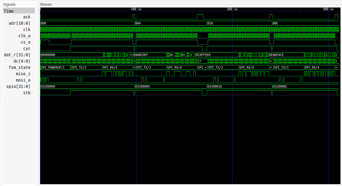
SPI Flash simulation results
Notice that the cs signal is inverted; you write a value of 1 to assert it, which pulls the corresponding pin low.
Finally, you can update the Memory_Test module and change how it is built and tested. The parent module only requires one small change, because the simulated memory and SPI Flash memory modules implement the same Wishbone bus specification. But the simulated memory module addresses 32-bit words of data, and SPI Flash addresses 8-bit bytes of data, so you should modify the line which increments the pc variable to add 4 instead of 1:
# Before:
m.d.sync += self.pc.eq( self.pc + 1 )
# After:
m.d.sync += self.pc.eq( self.pc + 4 )
Then, you can update the build and test logic to use a SPI_ROM module instead of a ROM module:
# Test program to run.
test_prog = [
  BLU_ON, DELAY( 5000000 ), GRN_ON, DELAY( 5000000 ),
  BLU_OFF, RED_ON, DELAY( 5000000 ), RED_OFF,
  DELAY( 10000000 ), GRN_OFF, DELAY( 5000000 ), RETURN
]
# 'main' method to simulate or build the test.
if __name__ == "__main__":
  # If the file was run with '-b', build for an iCE40UP5K breakout board
  if ( len( sys.argv ) == 2 ) and ( sys.argv[ 1 ] == '-b' ):
    offset = 2 * 1024 * 1024
    dut = Memory_Test( SPI_ROM( offset, offset + 1024, None ) )
    UpduinoV2Platform().build( dut )
  # If the file was run with '-w', write a binary file to write
  # to SPI Flash memory. (`iceprog -o 2M prog.bin`)
  elif ( len( sys.argv ) == 2 ) and ( sys.argv[ 1 ] == '-w' ):
    with open( 'prog.bin', 'wb' ) as f:
      for i in test_prog:
        f.write( bytes( [ ( i >> 0  ) & 0xFF,
                          ( i >> 8  ) & 0xFF,
                          ( i >> 16 ) & 0xFF,
                          ( i >> 24 ) & 0xFF ] ) )
  # If no arguments were passed in, simulate the design.
  else:
    offset = 2 * 1024 * 1024
    dut = Memory_Test( SPI_ROM( offset, offset + 1024, [
      BLU_ON, DELAY( 5 ), GRN_ON, DELAY( 5 ), BLU_OFF, RED_ON,
      DELAY( 10 ), RED_OFF, DELAY( 5 ), GRN_OFF, DELAY( 5 ), RETURN
    ] ) )
    with Simulator( dut, vcd_file = open( 'test.vcd', 'w' ) ) as sim:
      # Simulate running for 5000 clock cycles.
      def proc():
        for i in range( 5000 ):
          yield Tick()
          yield Settle()
      sim.add_clock( 1e-6 )
      sim.add_sync_process( proc )
      sim.run()
I also added a -w option to generate a program image to write to SPI Flash, since the new design will not have a built-in program to run. And you can still simulate this design, since the SPI_ROM module accepts an optional set of test data which it will simulate receiving:
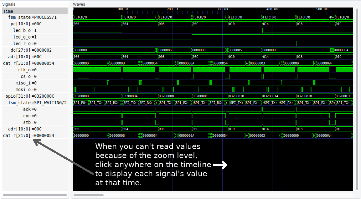
Checking the expected results of running a simple “program” from SPI Flash.
Once you’re happy with the simulation results, you can generate a binary image of the test program and write it to a 2 Megabyte offset in the board’s SPI Flash with:
python3 top.py -w
iceprog -o 2M prog.bin
Then, with a valid program image stored on the chip, you can write the design to your board:
python3 top.py -b
iceprog build/top.bin
The LEDs should cycle through various colors in time with the test program. If you change the test_prog array and re-build / re-write it, the LED color timings should change without making you re-flash the entire Test_Memory design.
Note that if you are using an Upduino board, it might take a few tries to re-write SPI memory once you upload a design which accesses the resource. If you see an error like this:
init..
cdone: low
reset..
cdone: high
Extended Device String Length is 0xFF, this is likely a read error. Ignorig...
flash ID: 0xFF 0xFF 0xFF 0xFF
file size: 104090
erase 64kB sector at 0x000000..
…or this:
erase 64kB sector at 0x000000..
erase 64kB sector at 0x010000..
programming..
reading..
Found difference between flash and file!
unexpected rx byte: 00
unexpected rx byte: 00
unexpected rx byte: 00
unexpected rx byte: 10
unexpected rx byte: 00
unexpected rx byte: 00
unexpected rx byte: 00
unexpected rx byte: 00
unexpected rx byte: 00
unexpected rx byte: 00
unexpected rx byte: 00
unexpected rx byte: 00
ABORT.
…or if the iceprog program freezes before it reads the flash ID, don’t panic! Your board isn’t bricked, you just tried to write to the board while the FPGA was busy accessing the SPI Flash. This doesn’t seem to happen on the Lattice evaluation board, which has a suspiciously similar schematic, so it could also be caused by EMI issues on the cheaper 2-layer PCB.
Whatever the reason, if you keep trying and occasionally un-plug the board and plug it back in again, you should eventually succeed in re-writing it. If you use longer DELAY(...) instructions, the FPGA will spend less time communicating with the Flash chip and it should be easier to re-program. You can also run iceprog -b to bulk-erase the entire Flash chip, but that command might also take a few tries to succeed.
Conclusions
From my inexperienced perspective, nMigen is a lot easier to use than Verilog or VHDL. A lot easier. It has its quirks, but you can learn a lot from the source code, which is pretty well-documented. The lack of actual documentation and tutorials is a little bit tricky, but I’ve found a few resources that are good starting points:
There’s also a very helpful #nmigen channel on Freenode IRC, which is where I learned a lot of the information presented here. So a huge thanks to those folks for helping me learn and getting me un-stuck while I whittle away these long hours.
All in all, if you’ve been wanting to try learning about hardware design and you’re not a fan of traditional hardware description languages, give nMigen a try!
DurandA
August 25, 2020 at 5:24 pm
I’d like to know more about your nMigen-based MCU.
Vivonomicon
September 6, 2020 at 1:10 pm
Well I wrote a post about it a few months ago, and it works well enough that I could port a simple “neopixel” LED project to run on it. But it’s a bit slow and it uses a lot of gates compared to other minimal RISC-V softcores, which means that you can’t fit too many peripherals into the 5,280 gates on an iCE40UP5K.
I would like to do some more work on it, but I’m taking a break until I get a chance to learn more about designing softcores, or a hobbyist-friendly FPGA comes out with more gates to work with, or nMigen/yosys add support for the iCE40UP5K’s 128KB of SPRAM.