Modern microcontrollers are amazing. They are much faster and cheaper than the sort of processors that powered “real” computers a few decades ago, and they’re also very power-efficient. But software complexity has also grown over time, and as we humans often say about ourselves as we age, it has grown in the wrong direction. Developers have gotten used to having enormous reserves of memory to draw from, so unless an application or library was specifically written for embedded platforms, it probably won’t be able to run with the scant kilobytes of RAM which are included in your average microcontroller.
Fortunately, most vendors include peripherals for accessing external memory when it is needed, and the STM32’s “Flexible Memory Controller” is surprisingly easy to use. Unfortunately, it is not easy to design a custom PCB with parallel memory modules. The interfaces use a lot of signals which are susceptible to electromagnetic noise, so it is important to ensure that all of the traces have the same length and impedance. This is especially hard on hobbyists, because 2-layer boards are not appropriate for these sorts of designs and KiCAD does not support length-matching for more than two traces yet.
So the target hardware for this tutorial will be a $40 STM32F723E Discovery Kit. It is a bit more expensive than the minimal “Nucleo” boards, but it includes 512KB of external RAM and a 240×240-pixel TFT display; we’ll learn how to drive both of those from the FMC peripheral in this post. It also includes 64MB of memory-mapped QSPI Flash memory, which I’ll talk about in a future post.
We’ll use the external RAM to store a framebuffer, which will be sent to the display using DMA.
This evaluation board uses BGA parts, which are almost impossible to solder without special equipment. But it provides an easy and affordable way to learn about writing software for these peripherals. When you are ready to use external memories in homemade designs, you can use QFP STM32s with at least 144 pins, TSSOP memory chips, and a 4-layer PCB.
FMC Overview
The STM32’s FMC peripheral can address a few different types of memory. There are four usable 256MB “banks” of internal memory space, each designed to access a specific memory technology. You can find this basic layout in the first two sections of the reference manual‘s “Flexible Memory Controller (FMC)” chapter. For our STM32F723IE chip, it looks like:
- Bank 1 @
0x60000000: Up to four NOR Flash, PSRAM, or SRAM chips with up to 64MB each. - Bank 2 @
0x70000000: Reserved (SDRAM can be remapped to this address). - Bank 3 @
0x80000000: NAND Flash. - Bank 4 @
0x90000000: Reserved (used by QSPI peripheral). - SDRAM Bank 1 @
0xC0000000: SDRAM. - SDRAM Bank 2 @
0xD0000000: SDRAM.
As you can see, Bank 2 is reserved and Bank 4 is not used by the FMC peripheral. Up to 512MB of SDRAM can be mapped to the two SDRAM banks, and Bank 3 is used exclusively for NAND Flash memory. Bank 1 is split into four 64MB areas which can each address a NOR Flash, PSRAM, or SRAM chip.
So you can see that the memory controller lives up to its name; it is flexible enough to adapt to a wide range of memory needs. It does not support DDR RAM, but SDRAM is very similar except for its lower speed, and not many STM32 chips are quick enough to use the faster DDR bus speeds anyways.
The FMC peripheral includes a lot of signals: there are data signals, address signals, read / write enable signals, “chip select” signals, and so on. The SDRAM banks also use separate control signals from the other FMC banks, i.e. FMC_SDNWE instead of FMC_NWE. You can see which signals should go to which pins on the memory module in the reference manual; the “SDRAM Controller” section describes the SDRAM signals, the “NAND Flash Controller” section describes the NAND signals, and so on. Our STM32F723 Discovery Kit includes a PSRAM chip with 16 data signals and 18 address lines, so let’s look at how the reference manual describes those signals:
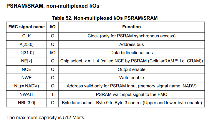
PSRAM FMC signal descriptions from the STM32F72xx reference manual.
You can look at the board’s schematics to see how those signals are connected; those are located in an appendix at the end of the discovery kit’s user manual:
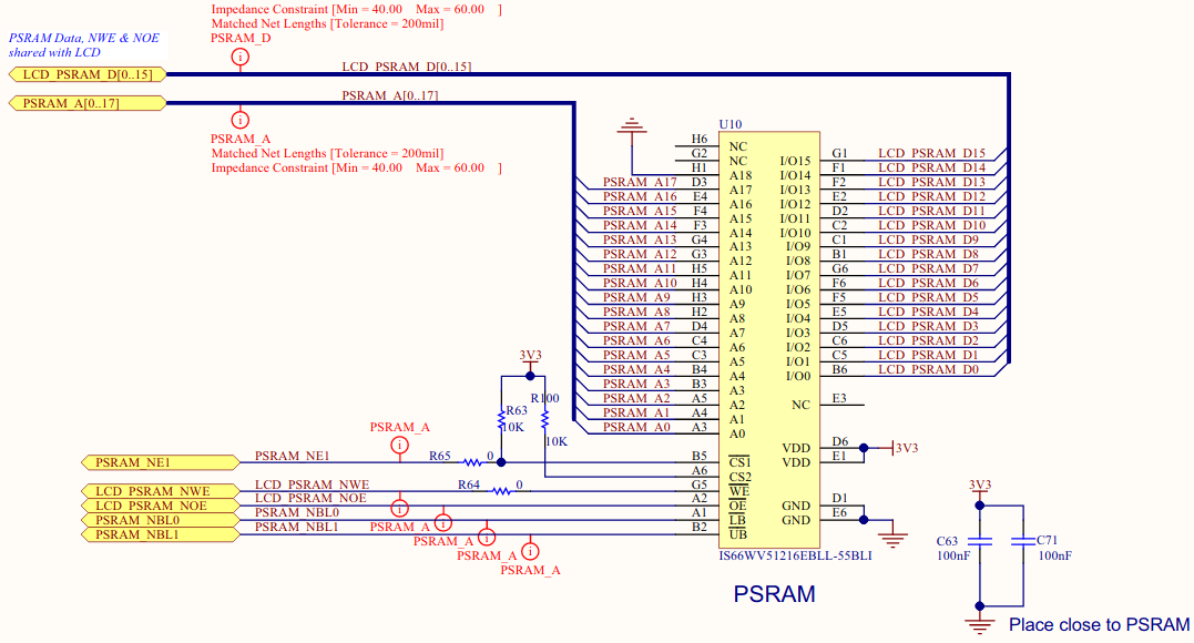
PSRAM schematic used by the STM32F723E Discovery Kit. This is actually a 1MB RAM chip, but we can only use 512KB because the A18 address pin is wired to Ground.
You can see that this PSRAM chip doesn’t use the CLK, NWAIT or NL signals; since it doesn’t use a clock signal, this will be treated as an asynchronous memory module. You can also see that the address and data lines need to have the same length +/- 200 mils with 40-60Ω impedance. (Remember, a “mil” is 1/1000 of an inch, not a millimeter).
The display is connected similarly, because a standard “8080” parallel TFT interface can use the same signals and interface as a PSRAM chip. The main difference is that only one address line is used, and it is connected to the display’s “data / command” pin. So we’ll only use two memory addresses to drive the display: one to send commands, and one to send data.
FMC Configuration
Fortunately, most of the FMC peripheral’s complexity lies in the hardware design. It can be difficult to make sure that the dozens of memory signals are all connected properly when you design a board, but it is fairly simple to write software to configure it once everything is in place. Luckily we’re using an official evaluation board, so we can be confident that the hardware is connected properly and focus on the software.
Clock and GPIO Setup
Before we actually use the external memory controller, we need to write some boilerplate code to set up the core system clock speed and connect the appropriate GPIO pins to the peripheral. I’ll omit some repetitive basics like the linker script and reset handler, but as usual, you can find example projects implementing this code on GitHub.
So first, let’s set the chip to its maximum recommended speed of 216MHz. When it powers on, a 16MHz internal oscillator is used to derive the core clock signal. But we can get a higher-speed signal by routing that 16MHz signal through the chip’s PLL module. The reference manual describes the PLL in the “Reset and Clock Control (RCC)” chapter, but tl;dr, you can generate a new clock frequency by setting a few values in the RCC registers:
PLL Frequency = ( Input * ( N / M ) / P )
In our case, the input value is 16MHz and we want an output frequency of 216MHz. To achieve that, I decided to set N = 54 and M = 2, with P staying at its default value of 2:
// (Somewhere globally accessible)
uint32_t SystemCoreClock = 16000000;

// (Near the top of your main method)
  // Set clock speed to 216MHz (each tick is a bit less than 5ns)
  // PLL out = ( 16MHz * ( N / M ) / P ). P = 2, N = 54, M = 2.
  FLASH->ACR   |=  ( 7 << FLASH_ACR_LATENCY_Pos );
  RCC->PLLCFGR &= ~( RCC_PLLCFGR_PLLN |
                     RCC_PLLCFGR_PLLM );
  RCC->PLLCFGR |=  ( ( 54 << RCC_PLLCFGR_PLLN_Pos ) |
                     ( 2 << RCC_PLLCFGR_PLLM_Pos ) );
  RCC->CR      |=  ( RCC_CR_PLLON );
  while ( !( RCC->CR & RCC_CR_PLLRDY ) ) {};
  RCC->CFGR    |=  ( 2 << RCC_CFGR_SW_Pos );
  while ( ( RCC->CFGR & RCC_CFGR_SWS ) != ( 2 << RCC_CFGR_SWS_Pos ) ) {};
  SystemCoreClock = 216000000;
I also set 7 wait-states in the internal Flash memory; you can find a table containing the recommended number of wait-states for a given clock speed and voltage range in the reference manual‘s “FLASH Functional Description” section.
Then we can enable the peripherals that we plan on using. In addition to the GPIO and FMC peripherals, we’ll use TIM5 to control the display’s brightness and USART6 to print information over a serial connection. We’ll also use DMA2 for moving data to the display from a framebuffer in the external RAM:
  // Enable peripheral clocks: GPIOA-H, TIM5, USART6, FMC, DMA2.
  RCC->AHB1ENR |=  ( RCC_AHB1ENR_GPIOAEN |
                     RCC_AHB1ENR_GPIOBEN |
                     RCC_AHB1ENR_GPIOCEN |
                     RCC_AHB1ENR_GPIODEN |
                     RCC_AHB1ENR_GPIOEEN |
                     RCC_AHB1ENR_GPIOFEN |
                     RCC_AHB1ENR_GPIOGEN |
                     RCC_AHB1ENR_GPIOHEN |
                     RCC_AHB1ENR_DMA2EN );
  RCC->AHB3ENR |=  ( RCC_AHB3ENR_FMCEN );
  RCC->APB1ENR |=  ( RCC_APB1ENR_TIM5EN );
  RCC->APB2ENR |=  ( RCC_APB2ENR_USART6EN );
Next, we need to configure the FMC pins with the appropriate alternate function settings. You can find a table describing the “alternate function” numbers for each pin at the end of Chapter 4 in the datasheet, and you can find a table describing how each GPIO pin is connected in Appendix A of the Discovery Kit user manual. To save you some trouble, the following pins are connected to the FMC peripheral on this board using alternate function #12:
B7, D0, D1, D4, D5, D7, D8, D9, D10, D11, D12, D14, D15, E0, E1, E7, E8, E9, E10, E11, E12, E13, E14, E15, F0, F1, F2, F3, F4, F5, F12, F13, F14, F15, G0, G1, G2, G3, G4, G5, G9.
Now you see why this peripheral is only included on packages with a lot of pins! To configure all of them, it’s not a bad idea to use a helper method. This isn’t the most efficient approach, but it makes the configuration code short enough to copy and paste here:
// Helper method to quickly configure a GPIO pin's
// mode, speed, and alternate function number.
void gpio_qconfig( GPIO_TypeDef* GPIOx, int pin,
                   int mode, int ospeed, int af ) {
  GPIOx->MODER      &= ~( 0x3    << ( pin * 2 ) );
  GPIOx->MODER      |=  ( mode   << ( pin * 2 ) );
  GPIOx->OSPEEDR    &= ~( 0x3    << ( pin * 2 ) );
  GPIOx->OSPEEDR    |=  ( ospeed << ( pin * 2 ) );
  if ( pin <= 7 ) {
    GPIOx->AFR[ 0 ] &= ~( 0xF    << ( pin * 4 ) );
    GPIOx->AFR[ 0 ] |=  ( af     << ( pin * 4 ) );
  }
  else {
    GPIOx->AFR[ 1 ] &= ~( 0xF    << ( ( pin - 8 ) * 4 ) );
    GPIOx->AFR[ 1 ] |=  ( af     << ( ( pin - 8 ) * 4 ) );
  }
}
In addition to the FMC pins, you’ll want to connect pins C6 and C7 to the USART6 peripheral, which is connected to the on-board debugger’s virtual serial port. Pin H7 is also connected to the display’s reset pin, and H11 controls its backlight brightness using PWM (Timer 5, channel 2):
  // Initialize GPIO pins for the appropriate peripherals.
  // C6, C7: USART6 TX/RX.
  gpio_qconfig( GPIOC, 6, 2, 2, 8 );
  gpio_qconfig( GPIOC, 7, 2, 2, 8 );
  // H7: Display reset, H11: Backlight brightness control.
  gpio_qconfig( GPIOH, 7, 1, 0, 0 );
  gpio_qconfig( GPIOH, 11, 2, 0, 2 );
  // FMC Pins: B7, D0, D1, D4, D5, D7, D8, D9, D10, D11, D12, D14,
  // D15, E0, E1, E7, E8, E9, E10, E11, E12, E13, E14, E15, F0, F1,
  // F2, F3, F4, F5, F12, F13, F14, F15, G0, G1, G2, G3, G4, G5, G9
  gpio_qconfig( GPIOB, 7, 2, 3, 12 );
  gpio_qconfig( GPIOD, 0, 2, 3, 12 );
  gpio_qconfig( GPIOD, 1, 2, 3, 12 );
  gpio_qconfig( GPIOD, 4, 2, 3, 12 );
  gpio_qconfig( GPIOD, 5, 2, 3, 12 );
  gpio_qconfig( GPIOD, 7, 2, 3, 12 );
  gpio_qconfig( GPIOD, 8, 2, 3, 12 );
  gpio_qconfig( GPIOD, 9, 2, 3, 12 );
  gpio_qconfig( GPIOD, 10, 2, 3, 12 );
  gpio_qconfig( GPIOD, 11, 2, 3, 12 );
  gpio_qconfig( GPIOD, 12, 2, 3, 12 );
  gpio_qconfig( GPIOD, 14, 2, 3, 12 );
  gpio_qconfig( GPIOD, 15, 2, 3, 12 );
  gpio_qconfig( GPIOE, 0, 2, 3, 12 );
  gpio_qconfig( GPIOE, 1, 2, 3, 12 );
  gpio_qconfig( GPIOE, 7, 2, 3, 12 );
  gpio_qconfig( GPIOE, 8, 2, 3, 12 );
  gpio_qconfig( GPIOE, 9, 2, 3, 12 );
  gpio_qconfig( GPIOE, 10, 2, 3, 12 );
  gpio_qconfig( GPIOE, 11, 2, 3, 12 );
  gpio_qconfig( GPIOE, 12, 2, 3, 12 );
  gpio_qconfig( GPIOE, 13, 2, 3, 12 );
  gpio_qconfig( GPIOE, 14, 2, 3, 12 );
  gpio_qconfig( GPIOE, 15, 2, 3, 12 );
  gpio_qconfig( GPIOF, 0, 2, 3, 12 );
  gpio_qconfig( GPIOF, 1, 2, 3, 12 );
  gpio_qconfig( GPIOF, 2, 2, 3, 12 );
  gpio_qconfig( GPIOF, 3, 2, 3, 12 );
  gpio_qconfig( GPIOF, 4, 2, 3, 12 );
  gpio_qconfig( GPIOF, 5, 2, 3, 12 );
  gpio_qconfig( GPIOF, 12, 2, 3, 12 );
  gpio_qconfig( GPIOF, 13, 2, 3, 12 );
  gpio_qconfig( GPIOF, 14, 2, 3, 12 );
  gpio_qconfig( GPIOF, 15, 2, 3, 12 );
  gpio_qconfig( GPIOG, 0, 2, 3, 12 );
  gpio_qconfig( GPIOG, 1, 2, 3, 12 );
  gpio_qconfig( GPIOG, 2, 2, 3, 12 );
  gpio_qconfig( GPIOG, 3, 2, 3, 12 );
  gpio_qconfig( GPIOG, 4, 2, 3, 12 );
  gpio_qconfig( GPIOG, 5, 2, 3, 12 );
  gpio_qconfig( GPIOG, 9, 2, 3, 12 );
You could make this even easier to read by creating human-readable macros for the “mode” and “output speed” values, but GPIO pin configuration is not what this post is about, so let’s move on. You can find a reference image explaining the different pin configuration fields in one of my earlier posts, and the reference manual’s “GPIO Registers” section is very legible.
Finally, we can initialize the USART6 peripheral for logging…
  // Setup USART6 for 115200-baud TX.
  USART6->BRR  =  ( SystemCoreClock / 115200 );
  USART6->CR1 |=  ( USART_CR1_UE | USART_CR1_TE );
…and implement printf over UART by creating a _write system call, like I talked about in my last post about the U[S]ART peripherals:
// System call to support standard library print functions.
int _write( int handle, char* data, int size ) {
  int count = size;
  while( count-- ) {
    while( !( USART6->ISR & USART_ISR_TXE ) ) {};
    USART6->TDR = *data++;
  }
  return size;
}
PSRAM Configuration
With the clock and GPIO pins configured, we can initialize the external memory peripheral. Let’s start with the PSRAM chip; if you look back to the schematic above, you can see that its “chip select” pin is connected to the FMC_NE1 signal. So we should configure the 1st section of “Bank 1” to address a PSRAM memory.
Each of the four NOR Flash / PSRAM sections use two configuration registers. The BCR register lets you configure what type of memory is connected and what features it supports, while the BTR register contains timing information which sets the memory access speed.
The first section of Bank 1 is configured for NOR Flash by default, so in the BCR register, we need to clear the FACCEN “Flash Access Enable” bit and set the MTYP “Memory Type” field to 1 for PSRAM. The first section of Bank 1 is also enabled by default, so we don’t need to set the MBKEN “Memory Bank Enable” bit. We can also leave the WREN “Write Enable” and MWID “Memory Bus Width” values alone, since they default to a 16-bit data bus writes enabled.
To set the access timings, we need to set the number of clock cycles to spend waiting at different points in a memory access cycle. Specifically, we’ll need to tell the peripheral how much time to spend in each of these phases:
BUSTURN: “Bus Turnaround” duration.DATAST: “Data Phase” duration.ADDSET: “Address Set” duration.ADDHLD: “Address Hold” duration.
These timing values are typically included in the memory module’s datasheet. These boards use an IS66WV51216 RAM chip with a -55 timing grade, which has these timing characteristics for a typical write cycle:
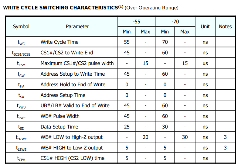
PSRAM write timings; the read timings are slightly different, but similar enough.
You can see that the names for different timings don’t quite match up with the values in the BTR register, but you can piece together a picture of how long you need to wait at different stages if you look at where each value goes in the “AC Waveforms” diagram:
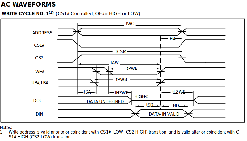
PSRAM write waveform. The values for each timing label are shown in the table above.
So it looks like the address setup and hold times are both zero nanoseconds – those are the tSA and tHA values. The “bus turnaround” time sets an extra delay when the peripheral moves from a read operation to a write operation, or vice-versa; I decided to look at the tLZWE value for that, which is 5ns. And the “data phase” duration is just the tWC “Write Cycle Time” of 55ns.
At a clock speed of 216MHz, each tick takes about 4.63ns, which I rounded up to 5ns. That means that the ADDSET and ADDHLD values can be set to 0, BUSTURN can be set to 1, and DATAST can be set to 11:
  // Initialize the memory controller for the connected PSRAM.
  // The 512KB of addressable RAM easily fits in the 64MB bank 1.
  // Bank 1 is enabled (but configured for NOR Flash) at reset.
  // So clear the 'flash enable' bit and set it to PSRAM mode.
  FMC_Bank1->BTCR[ 0 ] &= ~( FMC_BCR1_FACCEN |
                             FMC_BCR1_MTYP );
  FMC_Bank1->BTCR[ 0 ] |=  ( 1 << FMC_BCR1_MTYP_Pos );
  // Set access timings: 5ns bus turnaround, 55ns R/W cycle.
  FMC_Bank1->BTCR[ 1 ] &= ~( FMC_BTR1_BUSTURN |
                             FMC_BTR1_DATAST |
                             FMC_BTR1_ADDHLD |
                             FMC_BTR1_ADDSET );
  FMC_Bank1->BTCR[ 1 ] |=  ( ( 1 << FMC_BTR1_BUSTURN_Pos ) |
                             ( 11 << FMC_BTR1_DATAST_Pos ) );
The STM32 device header files lump the four groups of BCR and BTR registers into a BTCR array. BCR0 is BTCR[0], BTR0 is BTCR[1], BCR1 is BTCR[2], and so on.
With that done, you should be able to access the PSRAM just like internal RAM; it just starts at 0x60000000 instead of 0x20000000. You could add a PSRAM section to the linker script, but for this minimal example, I just created pointers to the PSRAM address and accessed them as arrays:
  // Test external RAM reads and writes.
  // Note: Uninitialized RAM can hold pseudorandom values.
  uint32_t* psram  = ( uint32_t* )0x60000000;
  uint16_t* psramh = ( uint16_t* )0x60000000;
  uint8_t*  psramb = ( uint8_t*  )0x60000000;
  printf( "RAM[0]: 0x%08lX (Uninitialized)\r\n", psram[ 0 ] );
  psram[ 0 ] = 0x01234567;
  psram[ 1 ] = 0x89ABCDEF;
  printf( "RAM[0]: 0x%02X (Byte)\r\n", psramb[ 0 ] );
  printf( "RAM[0]: 0x%04X (Halfword)\r\n", psramh[ 0 ] );
  printf( "RAM[0]: 0x%08lX (Word)\r\n", psram[ 0 ] );
  printf( "RAM[4]: 0x%08lX\r\n", psram[ 1 ] );
Depending on what kind of pointer you use to access the RAM, you can access it by byte, halfword, or word. When we set up a framebuffer for the 16bpp display, it will be convenient to use the uint16_t* pointer to address one pixel’s worth of data at a time.
If you build and run this example, you should see an output in the serial terminal that looks something like this. Remember, Cortex-M CPUs are little-endian, so the least-significant byte has the lowest address when you access bytes and halfwords:
RAM[0]: 0xAAAAAAAA (Uninitialized)
RAM[0]: 0x67 (Byte)
RAM[0]: 0x4567 (Halfword)
RAM[0]: 0x01234567 (Word)
RAM[4]: 0x89ABCDEF
And that’s all there is to it; from this point on, your code can treat the PSRAM as part of the STM32’s internal memory.
Notice that the RAM’s starting value is not zero; you shouldn’t make assumptions about the reset values of external RAM when your device first powers on. If you press the reset button without unplugging the board, the first uninitialized value will probably contain 0x01234567 because the RAM will retain previously stored data as long as it remains powered on. So when you write a real application, you might want to memset your external RAM to zero after your program initializes it.
This external RAM will also be slower than the STM32’s internal RAM; as we saw when we configured the bus timings, every access includes 12 clock cycles of waiting, which works out to a maximum access speed of about 18MHz. That’s fairly slow for RAM, but if you need high-performance external memory, SDRAM can run significantly faster than the PSRAM included on this evaluation board.
You can find an example project with this minimal PSRAM configuration code on GitHub.
Display Configuration
Next, we can set up the display. In addition to configuring the FMC peripheral, we’ll need to send a series of initialization commands and set up a DMA channel to transfer a framebuffer from the external RAM to the display.
FMC Setup
First, let’s set up the FMC peripheral. The display uses an ST7789 driver, which is very similar to the ILI9341 driver which I’ve written about previously. The timing characteristics for its parallel interface can be found in its datasheet:
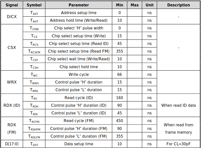
ST7789 timing values. Unlike most memory modules, reads take longer than writes!
These timing values are a little bit odd, as far as external memories go. A write cycle takes 66ns, but it takes 450ns to read pixel data! I’m going to ignore the read timings, since this example won’t ever need to read pixel data from the display. After all, we’ve got plenty of RAM for a framebuffer. 🙂
We can use a similar FMC configuration to that of the PSRAM chip. The display’s “chip select” pin is connected to the FMC_NE2 signal, so we should connect it to the 2nd section of “Bank 1”. This section is not enabled by default, so we’ll need to set the MBKEN bit in addition to clearing FACCEN and setting MTYP to 1 for PSRAM.
For the timing values, we can set ADDSET to 0 and ADDHLD to 2, matching the 0ns / 10ns values in the table above. The BUSTURN value can be set to 0, since we don’t expect to encounter read-to-write or write-to-read transitions; we’ll be writing all the time. And the DATAST duration can be set to 13, to set a write cycle time of about 65ns:
  // Initialize the memory controller for the connected TFT display.
  // It is connected to the 'NE2' signal, so use bank 1, section 2.
  FMC_Bank1->BTCR[ 2 ] &= ~( FMC_BCR2_FACCEN |
                             FMC_BCR2_MTYP );
  // Timings: 10ns address hold, 65ns write cycle.
  FMC_Bank1->BTCR[ 3 ] &= ~( FMC_BTR2_BUSTURN |
                             FMC_BTR2_DATAST |
                             FMC_BTR2_ADDHLD |
                             FMC_BTR2_ADDSET );
  FMC_Bank1->BTCR[ 3 ] |=  ( ( 13 << FMC_BTR2_DATAST_Pos ) |
                             ( 2 << FMC_BTR2_ADDHLD_Pos ) );
  FMC_Bank1->BTCR[ 2 ] |=  ( 1 << FMC_BCR2_MTYP_Pos |
                             FMC_BCR2_MBKEN );
Adding a Millisecond Delay Method
With the display interface configured, we need to write some initialization commands to turn it on and prepare it for drawing. Some of those commands, such as a software reset, require an extra delay to give the display time to process the command. So we’ll need a way to wait for a given number of milliseconds. The easiest way to do this is with the SysTick timer. ARM’s CMSIS header files provide a single function to enable this CPU peripheral and its associated interrupt. To generate 1ms ticks, you can call this after the code which configures a 216MHz clock speed:
SysTick_Config( SystemCoreClock / 1000 );
Then you can define a global uint32_t value called something like systick, and increment it in the SysTick interrupt handler:
// (Somewhere globally accessible)
volatile uint32_t systick = 0;

// SysTick interrupt handler: increment the global 'systick' value.
void SysTick_IRQn_handler( void ) {
  ++systick;
}
Finally, you can add a simple delay method which uses the systick value as a counter:
// Delay for a specified number of milliseconds.
void delay_ms( uint32_t ms ) {
  // Calculate the 'end of delay' tick value, then wait for it.
  uint32_t next = systick + ms;
  while ( systick < next ) { __WFI(); }
}
Although, that method is not completely bug-free; what would happen if you tried to delay for 1000ms when the 24-bit SysTick counter had a value of 0xFFFFFC? Code can be tricky like that.
Sending Initialization Commands
Now let’s move on to the actual display initialization. The display interface uses the same type of signals as a PSRAM memory, but it doesn’t have any address pins. Instead of writing pixel data to individual addresses, you send a series of commands which give it a rectangular area of the display to write to, followed by a stream of pixel colors.
The display does have a pin, usually labeled R/S, which determines whether incoming data should be treated as a command, or as data. The FMC peripheral’s “address 0” line is connected to this pin, and the second section of the FMC’s “Bank 1” starts at address 0x64000000. So when we write data to address 0x64000000, the R/S pin is held low and the data is treated as a command. And when we write data to address 0x64000002, the R/S pin is held high and the data is treated as…well, data.
You might wonder why 0x64000002 is used for display data instead of 0x64000001, when the “address 0” signal is used to toggle the pin. It’s because the data bus is 16 bits wide, so the address signals differentiate between halfwords instead of bytes.
So we can define two pointers to those addresses, and write to them whenever we want to address the display. But there’s a catch. If we frequently access external memory in a short period of time, there’s a chance that the chip will move too quickly or use stale data from its instruction or data cache. This isn’t very obvious when we only perform writes, but if you tried to read the display’s status registers immediately after sending a command which modifies them, you might get incorrect data back.
To avoid that, you can place memory barrier instructions after your reads and writes. These probably aren’t necessary for an example like this, but it’s good to be aware that these commands exist. You can read more about Cortex-M memory barriers in ARM’s documentation; I decided to place calls to __DSB(); and __ISB(); after each display memory transaction by placing a few macros in a tft.h header file:
#ifndef VVC_TFT_H
#define VVC_TFT_H

#include "global.h"

// Memory addresses used for display commands and data.
volatile uint16_t* tft_cmd;
volatile uint16_t* tft_dat;

// Macros to read / write TFT commands / data.
// These use memory barriers since the display is an external memory.
#define TFT_CMD( x ) \
  *tft_cmd = x; __DSB(); __ISB();
#define TFT_WR( x ) \
  *tft_dat = x; __DSB(); __ISB();
// Usage: `uint8_t var = TFT_RD();`
#define TFT_RD() \
  *tft_dat; __DSB(); __ISB();

// Helper method to send initialization commands to the TFT display.
void tft_init( void );
// Helper method to set the display drawing area to cover
// the entire 240x240-pixel screen.
void tft_draw_fullscreen();

#endif
Then you can put helper methods which use those macros, like this initialization sequence, in a tft.c source file:
#include "tft.h"

// Address bit 0 is used for the 'data / command' pin.
// (That's encoded as bit 1 in 16-bit mode)
volatile uint16_t* tft_cmd = ( volatile uint16_t* )0x64000000;
volatile uint16_t* tft_dat = ( volatile uint16_t* )0x64000002;

// Helper method to send initialization commands to the TFT display.
void tft_init( void ) {
  // Perform a hardware reset by toggling the display's reset pin.
  GPIOH->ODR &= ~( 1 << 7 );
  delay_ms( 100 );
  GPIOH->ODR |=  ( 1 << 7 );

  // Send 'software reset' command and wait for the display to reset.
  *tft_cmd = 0x01;
  delay_ms( 100 );

  // Send 'sleep out' command and wait for the display to wake up.
  *tft_cmd = 0x11;
  delay_ms( 100 );

  // Send 'display on' command.
  // Use memory barriers when delays aren't needed to ensure that
  // the external memory operation completes before proceeding.
  TFT_CMD( 0x29 );
  // Color mode: 16bpp.
  TFT_CMD( 0x3A );
  TFT_WR( 0x55 );
  // Display inversion "on". When this is off, 0x0000 = white...
  TFT_CMD( 0x21 );

  // Set the display drawing area.
  tft_draw_fullscreen();
}

// Helper method to set the display drawing area to cover
// the entire 240x240-pixel screen.
void tft_draw_fullscreen() {
  // Send the memory access commands.
  TFT_CMD( 0x2A );
  TFT_WR( 0x00 );
  TFT_WR( 0x00 );
  TFT_WR( 239 & 0xFF );
  TFT_WR( ( 239 >> 8 ) & 0xFF );
  TFT_CMD( 0x2B );
  TFT_WR( 0x00 );
  TFT_WR( 0x00 );
  TFT_WR( 239 & 0xFF );
  TFT_WR( ( 239 >> 8 ) & 0xFF );
  TFT_CMD( 0x2C );
}
You can find more information about individual commands in chapter 9 of the ST7789 datasheet. You can include those TFT files in your project and call tft_init(); after the FMC peripheral is initialized, but we need to do one more thing before you’ll see any results. Can you guess what it is?
Configuring Display Brightness
Yep, we need to turn on the display’s backlight. Remember that pin H11 connects to the display backlight circuit’s PWM input using Timer 5, Channel 2. We could have configured the pin as a push-pull output and pulled it high, but this board’s display has a surprisingly bright backlight. To compensate, I used a 10% duty cycle at 30KHz to make it dimmer:
  // Send display initialization commands.
  tft_init();

  // Turn on the display backlight @10% brightness, 30KHz PWM.
  // Calculate prescaler, compare, and autoreload values.
  uint32_t psc = 0;
  uint32_t arr = SystemCoreClock / 30000;
  if ( arr > 0xFFFF ) {
    psc = ( arr / 0xFFFF ) + 1;
    arr = arr / psc;
  }
  uint16_t ccr = ( uint16_t )( arr * 0.1 );
  TIM5->PSC    = psc;
  TIM5->ARR    = arr;
  TIM5->CCR2   = ccr;
  // Set the timer to "PWM mode 1" and enable it.
  TIM5->CCER  |=  ( TIM_CCER_CC2E );
  TIM5->CCMR1 &= ~( TIM_CCMR1_OC2M );
  TIM5->CCMR1 |=  ( 0x6 << TIM_CCMR1_OC2M_Pos );
  TIM5->EGR   |=  ( TIM_EGR_UG );
  TIM5->CR1   |=  ( TIM_CR1_CEN );
The board’s user manual actually recommends using a 1-10KHz PWM signal, but when I used that range of frequencies I heard an annoying inductor whine. 30KHz is much quieter.
If you include this timer configuration and the tft_init(); call from above in your program, you should be able to see the display light up with a rainbow of random colors when you build and run it:
TFT display immediately after initialization.
I’m worried that it might be a little hard to follow this post because I keep talking about inserting bits of code in different places. So before I talk about drawing to the display, if you’re having trouble seeing how this should all fit together, you can find an example project with this basic PSRAM and display initialization code on GitHub.
Setting up the Framebuffer and DMA Channel
Now that the display is initialized, let’s draw to it! The first step is to set up a framebuffer and configure a DMA channel to transfer data from that framebuffer to the display.
Setting up a framebuffer in external RAM is simple; we can access the psramh pointer that we defined earlier as an array:
  // Use the PSRAM as a display framebuffer; clear out an area of
  // 240*240*2 bytes (16 bits per pixel). Start with a purple color.
  // Color format is [MSb] R-G-B [LSb]. 5 bits for R and B, 6 for G.
  for ( int i = 0; i < ( 240 * 240 ); ++i ) {
    psramh[ i ] = 0x781F;
  }
The 16-bit colors are organized as 0bRRRRRGGGGGGBBBBB; 5 bits of red, 6 bits of green, and 5 bits of blue. So, 0x781F should be a blue-ish purple color; the most significant “red” bit and all of the “green” bits are set to zero. Once we have a full framebuffer, we can send it to the display with a one-time DMA transfer:
  // Configure the DMA peripheral to ferry display data from
  // PSRAM to the display in 'memory-to-memory' mode on stream 0.
  // (Note: DMA1 peripheral does not support memory-to-memory mode.)
  DMA2_Stream0->CR  |=  ( ( 2 << DMA_SxCR_PL_Pos ) |
                          ( 1 << DMA_SxCR_MSIZE_Pos ) |
                          ( 1 << DMA_SxCR_PSIZE_Pos ) |
                          DMA_SxCR_PINC |
                          ( 2 << DMA_SxCR_DIR_Pos ) );
  DMA2_Stream0->PAR  =  ( uint32_t )psramh;
  DMA2_Stream0->M0AR =  ( uint32_t )tft_dat;
  DMA2_Stream0->NDTR =  ( 240 * 240 );
  DMA2_Stream0->CR  |=  ( DMA_SxCR_EN );
  // Wait for the transfer to complete.
  while ( DMA2_Stream0->CR & DMA_SxCR_EN ) {};
  // Clear the 'transfer complete' flag.
  DMA2->LIFCR |=  ( DMA_LIFCR_CTCIF0 );
If you read my post about the STM32’s DMA peripheral, the STM32F7 line of chips have a “Type 2” DMA, which supports double-buffering but lacks a DMA multiplexer to let you choose which stream connects to which peripheral. No matter – the display and external RAM can both be accessed like normal memory, so we can use a “memory-to-memory” DMA transfer to send data from the framebuffer located in 0x60000000 – 0x6001C200 to the display data input located at 0x64000002.
Note that this chip’s DMA1 peripheral does not support memory-to-memory transfers, but DMA2 does. And when you configure a memory-to-memory transfer, the registers which usually refer to the “peripheral” side of the transaction refer the source, while the “memory” registers refer to the destination. So we set the PINC bit to increment the source address pointer after each transaction, but we leave the MINC bit cleared so that the destination address pointer remains the same. You also need to set the MSIZE and PSIZE fields to 1, for 16-bit data transfers.
If you build and run that code, the display should light up purple:
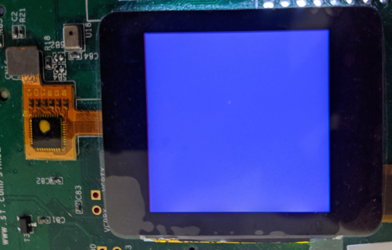
TFT displaying a solid blue / purple color.
But what if you want to draw more than a solid color?
Drawing to the Framebuffer
Now that we have a framebuffer, it’s pretty easy to write methods which draw points, lines, and rectangles to that area of memory. You might want to find a 3rd-party library for drawing to a framebuffer though, because that’s a common problem and it can be tedious to write efficient functions for things like drawing a line between two arbitrary points, or drawing text with good kerning.
But now that we have a fast and efficient way to transfer data from an external RAM chip to a display, you must be curious about how quickly the chip can refresh its display. So let’s set up a few simple drawing methods, and print a calculated Frames-PS value to the display itself.
Drawing Shapes
First, let’s set up some methods to draw pixels and rectangles. I used these function signatures in tft.h:
// TFT drawing functions. These draw to the framebuffer, so they
// will not be reflected on the display until the next refresh.
void tft_px( uint16_t* fb, int x, int y, uint16_t col );
void tft_hline( uint16_t* fb, int x, int y, int len, uint16_t col );
void tft_vline( uint16_t* fb, int x, int y, int len, uint16_t col );
void tft_rect( uint16_t* fb, int x, int y, int w, int h,
               int outline, uint16_t col );
Drawing a color to a single pixel is simple; make sure that it is not outside of the display area, then write the 16-bit color to the correct location in the framebuffer. Given X and Y coordinates on a 240×240-pixel display, the “array address” will be x + ( y * 240 ):
// Draw one pixel to the TFT framebuffer.
void tft_px( uint16_t* fb, int x, int y, uint16_t col ) {
  if ( ( x < 0 ) | ( x > 239 ) |
       ( y < 0 ) | ( y > 239 ) ) { return; }
  fb[ x + ( y * 240 ) ] = col;
}
Drawing horizontal and vertical lines is not much more complicated; you just draw a series of pixels in one direction, stopping early if the requested line length would extend past the display:
// Draw a horizontal line to the TFT framebuffer.
void tft_hline( uint16_t* fb, int x, int y, int l, uint16_t col ) {
  if ( ( x < 0 ) | ( x > 239 ) |
       ( y < 0 ) | ( y > 239 ) ) { return; }
  int len = l;
  if ( ( x + l ) > 239 ) { len = 240 - x; }
  for ( int xp = x; xp < ( x + len ); ++xp ) {
    fb[ xp + ( y * 240 ) ] = col;
  }
}

// Draw a vertical line to the TFT framebuffer.
void tft_vline( uint16_t* fb, int x, int y, int l, uint16_t col ) {
  if ( ( x < 0 ) | ( x > 239 ) |
       ( y < 0 ) | ( y > 239 ) ) { return; }
  int len = l;
  if ( ( y + l ) > 239 ) { len = 240 - y; }
  for ( int yp = y; yp < ( y + len ); ++yp ) {
    fb[ x + ( yp * 240 ) ] = col;
  }
}
You can draw rectangles with the same approach, but I also added an “outline” argument to this rectangle-drawing method. When it is zero, the method draws a filled rectangle. When it is greater than zero, the method draws a rectangular outline with edges N pixels wide:
// Draw a rectangle to the TFT framebuffer.
void tft_rect( uint16_t* fb, int x, int y, int w, int h,
               int outline, uint16_t col ) {
  if ( ( x < 0 ) | ( x > 239 ) |
       ( y < 0 ) | ( y > 239 ) ) { return; }
  int wd = w;
  int ht = h;
  if ( ( x + w ) > 239 ) { wd = 240 - x; }
  if ( ( y + h ) > 239 ) { ht = 240 - y; }
  if ( outline > 0 ) {
    // Draw a rectangle outline.
    int op;
    for ( op = y; op < ( y + outline ); ++op ) {
      tft_hline( fb, x, op, wd, col );
    }
    for ( op = ( y + ht - 1 ); op > ( y + ht - 1 - outline ); --op ) {
      tft_hline( fb, x, op, wd, col );
    }
    for ( op = x; op < ( x + outline ); ++op ) {
      tft_vline( fb, op, y, ht, col );
    }
    for ( op = ( x + wd - 1 ); op > ( x + wd - 1 - outline ); --op ) {
      tft_vline( fb, op, y, ht, col );
    }
  }
  else {
    // Draw a filled rectangle.
    if ( wd > ht ) {
      // Draw fewer horizontal lines than vertical ones.
      for ( int yp = y; yp < ( y + ht ); ++yp ) {
        tft_hline( fb, x, yp, wd, col );
      }
    }
    else {
      // Draw fewer (or ==) vertical lines than horizontal ones.
      for ( int xp = x; xp < ( x + wd ); ++xp ) {
        tft_vline( fb, xp, y, ht, col );
      }
    }
  }
}
This is all pretty basic, but drawing text can be a little more complicated.
Drawing Text
My method of drawing text is not the most efficient, but it works for simple applications. The basic idea is to define a 6×8 monospace font, which means that each character uses 48 pixels. That’s 48 bits of information, which means that two characters can be represented with three words of data. In practice, this means that I end up with a long list of values like this in a header file:
// Define a simple monospace font; each character is 6x8 pixels,
// which comes out to 6 bytes or 3 words for every 2 characters.
#define CH_A0       0x1F688868
#define CH_B0       0xFF898989
#define CH_A1B1     0x1F007600
#define CH_C0       0x7E818181
#define CH_D0       0xFF818181
#define CH_C1D1     0x66007E00
// (etc...)
#define CH_lct0     0x00081422
#define CH_rct0     0x00442810
#define CH_lct1rct1 0x00000000
The pixel data is ordered so that each byte represents one 8-pixel column. The most-significant byte, starting with the 32-bit value, represents the left-most column. So for the ‘A’ character’s values of 0x1F688868 and 0x1F00, that looks like:

Monospace ‘A’ hexadecimal font glyph.
To draw characters encoded this way, I use a few helper methods. First, a tft_glyph method accepts two words of font data, and draws only those bits which are set to 1 in a 6×8 rectangular area. It also accepts a “size” parameter, which will scale the font by drawing each font pixel as a square with sides of length “size”:
// Draw a 6x8 character glyph, defined across 48 bits of data.
// Only 'foreground' pixels are drawn.
void tft_glyph( uint16_t* fb, int x, int y, uint32_t w0, uint32_t w1,
                uint16_t col, int size ) {
  if ( ( x < 0 ) | ( x > 239 ) |
       ( y < 0 ) | ( y > 239 ) ) { return; }
  int px_incr = size;
  int line_h = 8 * size;
  int cur_x = x;
  int cur_y = y;
  for ( int wi = 31; wi >= 0; --wi ) {
    for ( int cx = cur_x; cx < ( cur_x + px_incr ); ++cx ) {
      for ( int cy = cur_y; cy < ( cur_y + px_incr ); ++cy ) {
        if ( w0 & ( 1 << wi ) ) {
          tft_px( fb, cx, cy, col );
        }
      }
    }
    cur_y += px_incr;
    if ( cur_y == ( y + line_h ) ) {
      cur_y = y;
      cur_x += px_incr;
    }
  }
  for ( int wi = 15; wi >= 0; --wi ) {
    for ( int cx = cur_x; cx < ( cur_x + px_incr ); ++cx ) {
      for ( int cy = cur_y; cy < ( cur_y + px_incr ); ++cy ) {
        if ( w1 & ( 1 << wi ) ) {
          tft_px( fb, cx, cy, col );
        }
      }
    }
    cur_y += px_incr;
    if ( cur_y == ( y + line_h ) ) {
      cur_y = y;
      cur_x += px_incr;
    }
  }
}
That function is called by a tft_char method which returns the 48 bits of font data which are associated with a given character. This is quite inefficient, because it uses a long chain of if / else statements. It would be better to store font data in something like a hash map, but this demonstration code is not intended for cutting-edge applications:
// Draw a character to the TFT framebuffer using the appropriate
// 48 bits of font data. See `global.h` for the font data.
void tft_char( uint16_t* fb, int x, int y, char c,
               uint16_t col, int size ) {
  if ( ( x < 0 ) | ( x > 239 ) |
       ( y < 0 ) | ( y > 239 ) ) { return; }
  uint32_t w0, w1;
  if ( c == 'A' ) {
    w0 = CH_A0;
    w1 = CH_A1B1 >> 16;
  }
  else if ( c == 'B' ) {
    w0 = CH_B0;
    w1 = CH_A1B1 & 0x0000FFFF;
  }
  // (etc...)
  else if ( c == '>' ) {
    w0 = CH_rct0;
    w1 = CH_lct1rct1 & 0x0000FFFF;
  }
  else {
    w0 = 0;
    w1 = 0;
  }
  tft_glyph( fb, x, y, w0, w1, col, size );
}
Finally, a short tft_text method accepts a null-terminated C string and draws each character to the display:
// Draw a null-terminated string of text to the TFT framebuffer.
// Text wrapping is not implemented.
// TODO: Take a 'string length' parameter instead?
void tft_text( uint16_t* fb, int x, int y, const char* str,
               uint16_t col, int size ) {
  if ( ( x < 0 ) | ( x > 239 ) |
       ( y < 0 ) | ( y > 239 ) ) { return; }
  int i = 0;
  int offset = 0;
  while( str[ i ] != '\0' ) {
    tft_char( fb, ( x + offset ), y, str[ i ], col, size );
    offset += 6 * size;
    ++i;
  }
}
I omitted most of the repetitive font data and tft_char method for the sake of brevity, but you can find those in the example project on GitHub. Sorry that these drawing methods are a bit rough around the edges, but I didn’t want to spend too much time writing about them because they aren’t really related to the external memory peripheral.
Calculating and Displaying FPS
Since I didn’t include all of the font data in the last section, you might want to copy at least part of the global.h, tft.h, and tft.c files from GitHub to use those drawing methods in your project.
If you want to avoid display artifacts like screen tearing, it’s easiest to update the framebuffer in between DMA transfers. Here’s an example main loop which draws a simple test pattern with colors that change over time:
  // Main loop.
  uint16_t col = 0;
  while( 1 ) {
    // Clear the framebuffer to the current 'color' value.
    for ( int i = 0; i < ( 240 * 240 ); ++i ) {
      psramh[ i ] = col;
    }

    // Draw a few test patterns.
    tft_text( psramh, 10, 100, "Hello world!\0", ( col ^ 0xFFFF ), 3 );
    tft_rect( psramh, 20, 20, 200, 60, 4, ( col ^ 0xFFFF ) );
    tft_rect( psramh, 30, 30, 180, 40, 3, ( col ^ 0xFFFF ) );
    tft_rect( psramh, 40, 40, 160, 20, 2, ( col ^ 0xFFFF ) );
    tft_rect( psramh, 20, 140, 200, 80, 0, ( col ^ 0xFFFF ) );

    // Increment the 'color' value.
    col += 1;

    // Reset the display drawing area.
    tft_draw_fullscreen();

    // Transfer the new framebuffer to the display.
    DMA2_Stream0->CR  |=  ( DMA_SxCR_EN );
    // Wait for the transfer to complete.
    while ( DMA2_Stream0->CR & DMA_SxCR_EN ) {};
    // Clear the 'transfer complete' flag.
    DMA2->LIFCR |=  ( DMA_LIFCR_CTCIF0 );
  }
Running that should put a few rectangles on the screen with a “Hello world” message, and the background and foreground should pulse through different colors as the program runs:
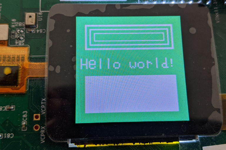
TFT displaying a test pattern.
The color transitions look pretty smooth to my eye, but it’s always nice to have numbers. So let’s calculate how many frames the chip can draw every second. For reference, movies have traditionally been shown at 24FPS, and most video games target 30-60FPS. Some enthusiasts use monitors which can display 90-144FPS, but 60FPS is a typical target for high-speed interactive applications.
To calculate how long our application takes to refresh the framebuffer and send it to the display, we can compare the systick values before and after a frame is drawn.
I decided to calculate FPS every other frame. On even frames, an a variable gets set to the current systick value. On odd frames, a b variable gets set to the current systick value. Since the values use milliseconds as a time unit, the framerate can be calculated as 1000 / ( b - a ):
  // Main loop.
  uint16_t col = 0;
  int a = 0;
  int b = 0;
  int fpsc = 0;
  float fps = 0.0;
  char fps_str[ 32 ] = "\0";
  while( 1 ) {
    // Calculate framerate every other frame.
    if ( fpsc ) {
      b = systick;
      fps = 1000.0 / ( float )( b - a );
      snprintf( fps_str, 32, "FPS: %.2f", fps );
    }
    else { a = systick; }
    fpsc = !fpsc;

    // Clear the framebuffer to the current 'color' value.
    for ( int i = 0; i < ( 240 * 240 ); ++i ) {
      psramh[ i ] = col;
    }

    // Draw a few test patterns, and the last calculated FPS.
    tft_text( psramh, 10, 100, "Hello world!\0", ( col ^ 0xFFFF ), 3 );
    tft_rect( psramh, 20, 20, 200, 60, 4, ( col ^ 0xFFFF ) );
    tft_rect( psramh, 30, 30, 180, 40, 3, ( col ^ 0xFFFF ) );
    tft_rect( psramh, 40, 40, 160, 20, 2, ( col ^ 0xFFFF ) );
    tft_rect( psramh, 20, 140, 200, 80, 0, ( col ^ 0xFFFF ) );
    tft_text( psramh, 30, 165, fps_str, col, 3 );

    // Increment the 'color' value.
    col += 1;

    // Reset the display drawing area.
    tft_draw_fullscreen();

    // Transfer the new framebuffer to the display.
    DMA2_Stream0->CR  |=  ( DMA_SxCR_EN );
    // Wait for the transfer to complete.
    while ( DMA2_Stream0->CR & DMA_SxCR_EN ) {};
    // Clear the 'transfer complete' flag.
    DMA2->LIFCR |=  ( DMA_LIFCR_CTCIF0 );
  }
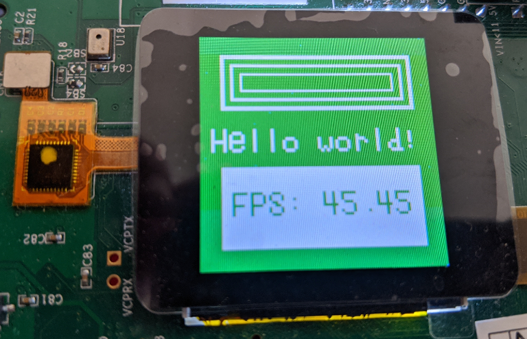
The snprintf standard library function lets you put a formatted string into a variable using the same syntax as printf. Here, the floating-point FPS value is printed with two decimal places of precision:
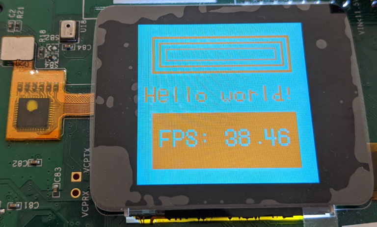
TFT with Frames-Per-Second display – it’s faster than 30FPS!
I get values of about 38FPS, which is pretty good for a microcontroller that fully refreshes the framebuffer between draw cycles. And I believe that you could go even faster on a board with SDRAM instead of PSRAM.
And again, you can find an example project with all of this FPS-drawing code on GitHub.
Overclocking the Interface
You can also try to go faster by reducing the wait times in the FMC peripheral, but this is risky. To demonstrate why it is risky, try reducing the DATAST value for both FMC configurations until you start to see…problems. You might be able to get the interface running stably at significantly higher speeds than it advertises:
Using shorter timing values in the BTR registers speeds things up, as you might expect.
…But you shouldn’t rely on those higher speeds without extensive testing. The datasheets describe stable operating parameters, and while you can often run devices faster than advertised, those operating conditions might not be stable. The devices might work fine in a narrow temperature range, or in environments which don’t have much electromagnetic noise, but if you design a consumer device with overclocked modules, those devices might fail prematurely or stop working in real-world conditions like a hot and humid day.
With a display, you can sometimes see the point where an interface can almost, but not quite keep up. In my case, a DATAST value of 3 for both PSRAM and display seems to land near that border:
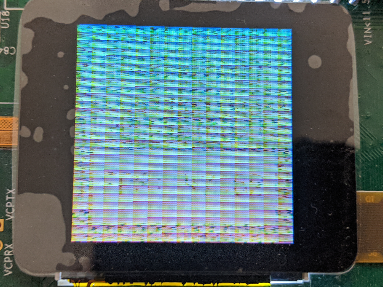
Speeding things up too much can cause problems.
If you look closely, you can see that it’s trying to draw a rectangle with text in the bottom half of the display, but it’s obvious that the interface is not working properly.
You can also overclock the STM32 chip itself by mis-configuring the PLL, which I’ve briefly talked about before. If you used an N value of 60 instead of 54 to configure the PLL in this example’s clock configuration code, the chip would run at 240MHz instead of 216MHz. And sure enough, when I make that change and set the SystemCoreClock value to 240,000,000, everything seems to work fine. The memories end up being slightly overclocked because, for example, 13 ticks at 240MHz is 54ns instead of 60ns. But with the faster CPU and bus speeds, the display reports 43FPS instead of 38FPS.
Still, I wouldn’t want to design a product with that 240MHz clock speed unless I really needed to, because ST’s reference materials repeatedly tell you not to run the chip faster than 216MHz. Even though it seems to work fine, it might cause overheating issues, or break certain types of peripherals, or occasionally read the wrong value from memory, or it might only work on “high-quality” chips which happen to have very few imperfections in their silicon die.
Conclusions
I had a lot of fun learning about the FMC peripheral and writing this post. The task of designing hardware with external memories seems daunting, but I was pleasantly surprised by how easy it was to write software for the external memory controller. And having a color display that can comfortably refresh at 30FPS opens up a lot of possibilities.
I don’t know if I’ll have time to pursue those possibilities (busy, busy, busy), but it’s still exciting to see how easy it is to mitigate memory constraints, which are one of the biggest obstacles to using fast microcontrollers for non-trivial tasks.
And speaking of non-trivial tasks, the mainline Linux kernel has started to support embedded targets like Xtensa and ARM Cortex-M chips, if they have at least several megabytes of RAM. It looks like there are a few limitations because the chips lack an MMU, but I bet you could make a single-board computer with an STM32F7, an SD card slot, and 16MB+ of SDRAM. I wonder how much you’d be able to realistically accomplish with a board like that. Probably not a whole lot, and there’s no way it would be competitive with a $10 Rasperry Pi Zero W, but it might be fun to investigate.
Anyways, I hope this was educational; questions and comments are welcome as always.