
If I had to guess what the world’s most popular footprint for low-density memory chips was, I would probably be wrong. But I’ll bet that the humble 8-pin SOIC / DIP / DFN formats would be near the top. You’ve probably used these before; most ESP8266 and ESP32 modules have one under their little metal shield, and motherboards for computers / cars / synthesizers / etc. often use them for storing UEFI / BIOS / firmware configurations and suchlike.
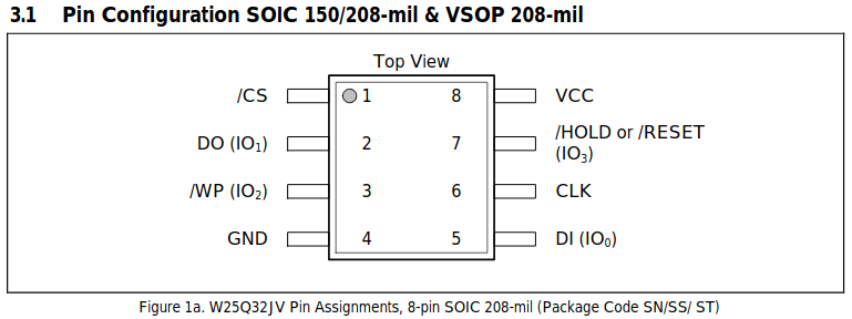
Pin assignments for a generic Flash module (Winbond W25Q series)
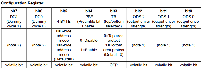
You can get RAM, Flash, EEPROM, and even FRAM memory in these common 8-pin packages. They usually use a SPI interface for communication, with a couple of extra pins for functions like write protection or suspending an ongoing transaction. But if you look in the image above, you’ll see that the /WP “Write Protect” and /HOLD or /RESET wires are also marked as IO2 and IO3. That’s because many 8-pin Flash chips also support a “Quad-SPI” interface, which is very similar to a bidirectional “3-wire” SPI interface, except that it has four I/O wires instead of one.
Some STM32 chips include a QSPI peripheral to interface with these kinds of Flash memory chips. You can use it to manually configure / erase / program the Flash chip, and once it’s initialized, you can also map the external Flash as read-only memory in the STM32’s internal memory space. The peripheral supports prefetching, caching, executing code, and it can even access two QSPI Flash chips in parallel, using 8 data lines in total to transfer a full byte of data every clock cycle.
To learn about the QSPI peripheral, I used the same STM32F723E Discovery Kit from my last post about external memories. In addition to its external RAM and display, this board includes one 64MB QSPI Flash chip connected to the QSPI peripheral. In this post, we’ll learn how to configure the Flash chip for quad I/O access, erase a sector, and write some test values. Then we’ll set the QSPI peripheral to its read-only “memory-mapped” mode, and read those test values by accessing the chip’s internal memory space starting at 0x90000000. If you don’t like copy/pasting, you can find an example project with this code on GitHub.
It is a little bit annoying that you can’t write to the Flash chip in memory-mapped mode, but this peripheral still presents a simple way to quickly read from external Flash using only six I/O pins. And writing to Flash memory has some unique limitations anyways, which is why it is often used to store data which an application rarely needs to modify, like firmware or audio/visual resources. So if you want to learn how to use Quad-SPI Flash memories with an STM32, read on!
QSPI Overview
The QSPI peripheral can be configured for one of four “modes” at any given time. They are:
- Indirect write mode: This mode performs manual QSPI write transactions.
- Indirect read mode: This mode performs manual QSPI read transactions.
- Status flag polling mode: This mode automatically reads a status register from the Flash chip until a specified set of flags are set and/or cleared. It can be used to wait for long operations such as sector erases to complete.
- Memory-mapped mode: This mode mounts the Flash chip as read-only memory in the STM32’s internal memory space.
To initialize the chip or perform an erase / write sequence, you can use the indirect write mode to send commands, followed by the status flag polling mode to wait for the Flash chip to finish processing those commands. And to read data from the Flash chip after it has been initialized and programmed, you can use the memory-mapped mode. But if your Flash chip is larger than the 256MB of internal memory space dedicated to the QSPI peripheral, you’ll need to use the indirect read mode to read data which is located after the first 256MB.
Each read and write operation is also split into five “phases”. It will be easier to explain each phase if you look at this waveform diagram from the reference manual first:
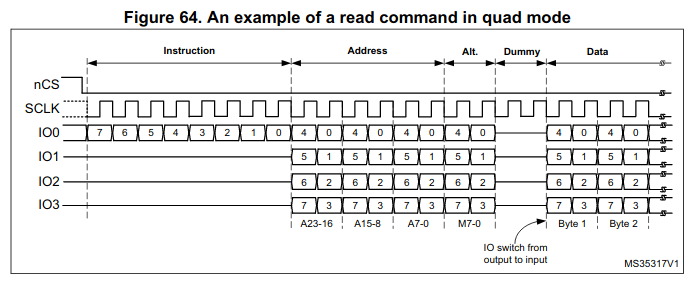
QSPI transaction phases, as the peripheral defines them.
Each phase corresponds with part of a typical QSPI memory transaction. First is the “instruction phase”, which sends an 8-bit instruction to the chip. This could be a simple command like 0x06 (“Enable Writes”), in which case only the “instruction” phase is used. Or it could be a memory access command like 0xEC (“Quad I/O Read with 4-byte addressing”), in which case the “instruction”, “address”, “dummy”, and “data” phases are all required. “Dummy cycles” are used to give the chip time to prepare its response with high-speed Quad-I/O accesses, and I don’t think that the “alternate bytes” phase is used by the Flash chip included on this board.
You can find a table of commands and descriptions of what they do in your memory chip’s datasheet; the STM32F723E Discovery Kit uses a Micron MX25L51245G Flash chip. Most 8-pin Flash chips use 24-bit addressing by default, but since this one contains more than 16MB of memory, it also supports 32-bit addressing.
Different commands have different address and data byte requirements, so you can enable or disable each phase individually. You can also set each phase to use a different number of data lines; in the figure above, the “instruction phase” only uses one data line, while the other phases use four. But MX25L512 chips support 4-wire instructions, so after we issue the 0x35 “Enable Quad I/O” command, we can use 4 data lines for every phase.
Boilerplate: Configure Clocks, GPIO Pins, etc.
We can use the same clock configuration code from my last post to set a core clock speed of 216MHz. The peripheral would work fine at the default speed of 16MHz, but then I wouldn’t have an excuse to talk about configuring the QSPI peripheral for a max speed of 84MHz:
  // Set clock speed to 216MHz (each tick is a bit less than 5ns)
  // PLL out = ( 16MHz * ( N / M ) / P ). P = 2, N = 54, M = 2.
  FLASH->ACR   |=  ( 7 << FLASH_ACR_LATENCY_Pos );
  RCC->PLLCFGR &= ~( RCC_PLLCFGR_PLLN |
                     RCC_PLLCFGR_PLLM );
  RCC->PLLCFGR |=  ( ( 54 << RCC_PLLCFGR_PLLN_Pos ) |
                     ( 2 << RCC_PLLCFGR_PLLM_Pos ) );
  RCC->CR      |=  ( RCC_CR_PLLON );
  while ( !( RCC->CR & RCC_CR_PLLRDY ) ) {};
  RCC->CFGR    |=  ( 2 << RCC_CFGR_SW_Pos );
  while ( ( RCC->CFGR & RCC_CFGR_SWS ) != ( 2 << RCC_CFGR_SWS_Pos ) ) {};
  SystemCoreClock = 216000000;
The Discovery Kit’s user manual shows that pins B2, B6, C9, C10, D13, and E2 are connected to the QSPI peripheral, so we’ll need to enable the GPIOB, GPIOC, GPIOD, and GPIOE peripherals in addition to QUADSPI. USART6 is also used for printing messages over the board’s serial connection:
  // Enable peripheral clocks: GPIOB-E, QSPI, USART6.
  RCC->AHB1ENR |=  ( RCC_AHB1ENR_GPIOBEN |
                     RCC_AHB1ENR_GPIOCEN |
                     RCC_AHB1ENR_GPIODEN |
                     RCC_AHB1ENR_GPIOEEN );
  RCC->AHB3ENR |=  ( RCC_AHB3ENR_QSPIEN );
  RCC->APB2ENR |=  ( RCC_APB2ENR_USART6EN );
The STM32F723IE datasheet shows that pin B6 uses alternate function #10 for QSPI, while the other pins use alternate function #9. Pin B6 should also be configured with a pull-up resistor, since it is connected to the “chip select” pin which activates the Flash memory when it is held low. There is also a pull-up resistor soldered to the board, but you might be able to omit that part from your designs if you configure the chip’s internal pull-up in your code:
  // Initialize pins C6 and C7 for USART6.
  GPIOC->MODER    |=  ( ( 2 << ( 6 * 2 ) ) |
                        ( 2 << ( 7 * 2 ) ) );
  GPIOC->OSPEEDR  |=  ( ( 2 << ( 6 * 2 ) ) |
                        ( 2 << ( 7 * 2 ) ) );
  GPIOC->AFR[ 0 ] |=  ( ( 8 << ( 6 * 4 ) ) |
                        ( 8 << ( 7 * 4 ) ) );
  // Initialize pins B2, B6, C9, C10, D13, E2 for QSPI.
  GPIOB->MODER    |=  ( ( 2 << ( 2 * 2 ) ) |
                        ( 2 << ( 6 * 2 ) ) );
  GPIOB->OSPEEDR  |=  ( ( 3 << ( 2 * 2 ) ) |
                        ( 3 << ( 6 * 2 ) ) );
  GPIOB->PUPDR    |=  ( 1 << ( 6 * 2 ) );
  GPIOB->AFR[ 0 ] |=  ( ( 9 << ( 2 * 4 ) ) |
                        ( 10 << ( 6 * 4 ) ) );
  GPIOC->MODER    |=  ( ( 2 << ( 9 * 2 ) ) |
                        ( 2 << ( 10 * 2 ) ) );
  GPIOC->OSPEEDR  |=  ( ( 3 << ( 9 * 2 ) ) |
                        ( 3 << ( 10 * 2 ) ) );
  GPIOC->AFR[ 1 ] |=  ( ( 9 << ( ( 9 - 8 ) * 4 ) ) |
                        ( 9 << ( ( 10 - 8 ) * 4 ) ) );
  GPIOD->MODER    |=  ( 2 << ( 13 * 2 ) );
  GPIOD->OSPEEDR  |=  ( 3 << ( 13 * 2 ) );
  GPIOD->AFR[ 1 ] |=  ( 9 << ( ( 13 - 8 ) * 4 ) );
  GPIOE->MODER    |=  ( 2 << ( 2 * 2 ) );
  GPIOE->OSPEEDR  |=  ( 3 << ( 2 * 2 ) );
  GPIOE->AFR[ 0 ] |=  ( 9 << ( 2 * 4 ) );
Pins C6 and C7 are also connected to USART6, and I also added the usual _write method to enable the printf standard library function; you can find that in the example project on GitHub or in my post about UART communication.
QSPI Configuration
The QSPI peripheral only needs a few pieces of information to start communicating with a Flash chip. First, we need to tell it how large the connected memory is. The DCR register contains an FSIZE (“Flash Size”) field which holds that information. It expects an exponent value:
#Bytes = 2 ^ (FSIZE + 1)
In our case, 64MB = 2 ^ 26 Bytes, so FSIZE = 25. Next, we should configure the transaction phases: setting the IMODE field to 1 in CCR enables the “instruction phase” with one data wire. I also configured the ADSIZE field for 32-bit addressing, because I’ll issue the 0xB7 “enable 4-byte addressing” command before performing any memory accesses:
  // QSPI peripheral initialization.
  // Set Flash size; 512Mb = 64MB = 2^(25+1) bytes.
  QUADSPI->DCR |=  ( 25 << QUADSPI_DCR_FSIZE_Pos );
  // Set 1-wire data mode with 32-bit addressing.
  QUADSPI->CCR |=  ( ( 3 << QUADSPI_CCR_ADSIZE_Pos ) |
                     ( 1 << QUADSPI_CCR_IMODE_Pos ) );
We’ll also need to set a clock prescaler; the Flash chip’s datasheet contains a “Dummy Cycle and Frequency Table” which defines how quickly the interface can run with different numbers of dummy cycles. The default number of dummy cycles is 6 for the “Quad I/O Fast Read” command, which corresponds with a 84MHz top speed. Setting the PRESCALER field to 2 will give us a frequency of 216MHz / (2+1) = 72MHz, which is close enough for this example:
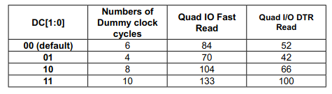
QSPI dummy cycles table from the Flash chip’s datasheet.
It’s also a good idea to set the SSHIFT bit in the peripheral’s control register. That tells the peripheral to wait an extra half clock cycle before reading values from the Flash chip, which seems to help account for signal delays and noise.
Once the peripheral is configured, you can set the EN bit to enable it:
  // Wait an extra half-cycle to read, and set a clock prescaler of 2+1=3.
  QUADSPI->CR  |=  ( QUADSPI_CR_SSHIFT |
                     ( 2 << QUADSPI_CR_PRESCALER_Pos ) );
  // Enable the peripheral.
  QUADSPI->CR  |=  ( QUADSPI_CR_EN );
Initialization
Once the peripheral is set up, you can start sending commands to initialize the Flash chip. Since we only set the IMODE field in the CCR register, only the instruction phase is enabled. The first order of business is to send the 0x35 “Enable Quad I/O” command to the chip, which will let us use all four data wires instead of one:
  // Set the 'enter QSPI mode' instruction.
  QUADSPI->CCR |=  ( 0x35 << QUADSPI_CCR_INSTRUCTION_Pos );
  // Wait for the transaction to complete, and disable the peripheral.
  while ( QUADSPI->SR & QUADSPI_SR_BUSY ) {};
  QUADSPI->CR  &= ~( QUADSPI_CR_EN );
As you might guess, the INSTRUCTION field in the CCR “Communication Configuration Register” contains the 8-bit instruction to send to the chip. And when you are using the indirect and status-polling modes, it’s a good idea to disable the QSPI peripheral when you aren’t using it. When it is active, the peripheral will automatically start a new transaction when certain fields or registers are written, depending on which phases are enabled.
With only the “instruction phase” enabled, the reference manual says that a new transaction will start whenever the INSTRUCTION field is modified. I don’t know whether clearing the field counts as modifying it, but I figure it’s better to be safe than sorry. And when multiple phases are enabled, writing to the “last” active configuration field (instruction -> address -> data) starts the transaction. That can get confusing, so to avoid accidentally starting a transaction, I decided to only enable the peripheral right before a new transaction should start.
Next, we need to wait for the Flash chip to acknowledge our request. We can do that by checking its status registers; some commands will cause the chip to respond with some basic information about its current state. In this case, we want to check the main status register, which is returned by the 0x05 “read status register” command. If bit #6 is set in the response, then the chip is in QSPI mode. It’s also a good idea to check bit #1, which is the “write in progress” bit; if that bit is set, the chip is busy writing and you should wait for it to finish:
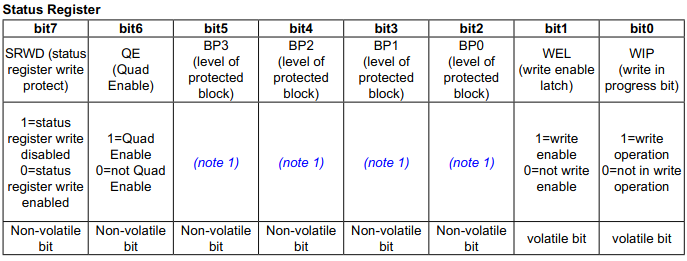
QSPI status register bits. We’ll mostly be interested in the “Quad Enable”, “Write Enable Latch”, and “Write in Progress” bits.
This sort of situation is what the peripheral’s “status flag polling mode” is for. It accepts a “mask” value which tells it which bits to pay attention to, and a “match” value which tells it what those bits should be set to. We want to wait for the status register to have bit #6 set and bit #1 cleared, so we can set a “mask” value of 0x41 and a “match” value of 0x40. Since “wait for value X in register Y” is a common task, I decided to write a helper method:
// Use 'status-polling' mode to wait for Flash register status.
void qspi_reg_wait( uint8_t reg, uint32_t msk, uint32_t mat ) {
  // Disable the peripheral.
  QUADSPI->CR   &= ~( QUADSPI_CR_EN );
  // Set the 'mask', 'match', and 'polling interval' values.
  QUADSPI->PSMKR = msk;
  QUADSPI->PSMAR = mat;
  QUADSPI->PIR   = 0x10;
  // Set the 'auto-stop' bit to end the transaction after a match.
  QUADSPI->CR   |=  ( QUADSPI_CR_APMS );
  // Clear instruction, mode and transaction phases.
  QUADSPI->CCR  &= ~( QUADSPI_CCR_INSTRUCTION |
                      QUADSPI_CCR_FMODE |
                      QUADSPI_CCR_IMODE |
                      QUADSPI_CCR_DMODE |
                      QUADSPI_CCR_ADMODE );
  // Set 4-wire instruction and data modes, and auto-polling mode.
  QUADSPI->CCR  |=  ( ( 3 << QUADSPI_CCR_IMODE_Pos ) |
                      ( 3 << QUADSPI_CCR_DMODE_Pos ) |
                      ( 2 << QUADSPI_CCR_FMODE_Pos ) );
  // Enable the peripheral.
  QUADSPI->CR   |=  ( QUADSPI_CR_EN );
  // Set the given 'read register' instruction to start polling.
  QUADSPI->CCR  |=  ( reg << QUADSPI_CCR_INSTRUCTION_Pos );
  // Wait for a match.
  while ( QUADSPI->SR & QUADSPI_SR_BUSY ) {};
  // Acknowledge the 'status match flag.'
  QUADSPI->FCR |=  ( QUADSPI_FCR_CSMF );
  // Un-set the data mode and disable auto-polling.
  QUADSPI->CCR  &= ~( QUADSPI_CCR_FMODE |
                      QUADSPI_CCR_DMODE );
  // Disable the peripheral.
  QUADSPI->CR   &= ~( QUADSPI_CR_EN );
}
Like I said earlier, it’s good to have the peripheral rest in an “off” state when you are using “indirect” or “status flag polling” modes, so I have logic to disable it at the start and end of the method. The “mask” and “match” values are set near the top, along with a “polling interval” value which tells the peripheral how often it should read its register from the Flash chip.
The APMS bit causes the peripheral to set the BUSY flag and stop requesting new values when it gets a match, which is the behavior that we want. And since the response is sent during the data phase, we need to set both instruction and data phases to use all four data lines. We also need to set the FMODE field to 2, which enables the status flag polling mode.
Once all of that is done, we can enable the peripheral and wait for the BUSY flag to be set. Once it is, we need to set the CSMF “clear status match” flag in the FCR “Flag Clear Register” to acknowledge the match. With that method in place, we can add logic to wait for the Flash chip to enable its QSPI functionality after sending the 0x35 instruction:
  // Wait for the 'QSPI mode enabled' bit.
  qspi_reg_wait( 0x05, 0x41, 0x40 );
Then we can enable 4-byte addressing mode to use 32-bit addresses instead of 24-bit ones using the same sort of logic. We just send the 0xB7 command instead of 0x35, and we wait for bit #5 in the “configuration register” returned by the 0x15 command:
QSPI configuration register; we only care about the “4BYTE” bit in this example.
  // Send 'enable 4-byte addressing' command.
  // The peripheral may start a new transfer as soon as the
  // 'instruction' field is written, so it is safest to disable
  // the peripheral before clearing that field.
  while ( QUADSPI->SR & QUADSPI_SR_BUSY ) {};
  QUADSPI->CR  &= ~( QUADSPI_CR_EN );
  QUADSPI->CCR &= ~( QUADSPI_CCR_INSTRUCTION );
  // Use all 4 data lines to send the instruction.
  QUADSPI->CCR |=  ( 3 << QUADSPI_CCR_IMODE_Pos );
  // Enable the peripheral and send the 'enable 4B addresses' command.
  QUADSPI->CR  |=  ( QUADSPI_CR_EN );
  QUADSPI->CCR |=  ( 0xB7 << QUADSPI_CCR_INSTRUCTION_Pos );
  // Wait for the transaction to complete, and disable the peripheral.
  while ( QUADSPI->SR & QUADSPI_SR_BUSY ) {};
  QUADSPI->CR  &= ~( QUADSPI_CR_EN );
  // Wait for the '4-byte addressing enabled' bit to be set.
  qspi_reg_wait( 0x15, 0x20, 0x20 );
With those two configuration commands sent, we are finally ready to write data to the chip.
Erasing a Sector
Flash chips are harder to write to than RAM chips, because they cannot perform random single-byte writes. The chip can clear individual bits of data, but the only way it can set bits is through a bulk erase operation. When you erase a sector of memory, all of the bits in that sector are set to 1. After that is done, you can “write” data by clearing any bits which need to be 0. But once you’ve cleared a bit, it can only be set again by erasing its entire sector.
Flash memory can also only survive a limited number of erase cycles before it stops working. The approximate number of erase cycles that each sector can handle is called “write endurance”.
Those complications mean that the QSPI peripheral’s “memory-mapped” mode cannot perform writes. If you wanted to write 0x12 followed by 0x34 to the same address, you would need to erase and restore an entire sector of memory, changing only the one byte which you were interested in. That would take a long time, and if it happened frequently in the background, you might unknowingly burn out the Flash chip by using up its limited number of erase cycles.
So when you want to write data, you’ll need to use the peripheral’s “indirect” and “status flag polling” modes. To erase a sector, we first need to send the 0x06 “enable writes” command and wait for the corresponding configuration register flag to be set:
// Enable writes on the QSPI Flash. Must be done before every
// erase / program operation.
void qspi_wen() {
  // Disable the peripheral.
  QUADSPI->CR   &= ~( QUADSPI_CR_EN );
  // Clear the instruction, mode, and transaction phases.
  QUADSPI->CCR  &= ~( QUADSPI_CCR_INSTRUCTION |
                      QUADSPI_CCR_FMODE |
                      QUADSPI_CCR_IMODE |
                      QUADSPI_CCR_DMODE |
                      QUADSPI_CCR_ADMODE );
  // Set 4-wire instruction mode.
  QUADSPI->CCR  |=  ( 3 << QUADSPI_CCR_IMODE_Pos );
  // Enable the peripheral and send the 'write enable' command.
  QUADSPI->CR  |=  ( QUADSPI_CR_EN );
  QUADSPI->CCR |=  ( 0x06 << QUADSPI_CCR_INSTRUCTION_Pos );
  // Wait for the transaction to finish.
  while ( QUADSPI->SR & QUADSPI_SR_BUSY ) {};
  // Disable the peripheral.
  QUADSPI->CR   &= ~( QUADSPI_CR_EN );
  // Wait until 'writes enabled' is set in the config register.
  qspi_reg_wait( 0x05, 0x43, 0x42 );
}
Then, we can create a helper method which calls that function and sends the 0x20 “erase sector” command. We also need to give it the address of the sector that we want to erase, which needs to be aligned to the size of a sector (4KB in this chip). So we need to enable the “instruction” and “address” phases with 4 data lines each:
// Erase a 4KB sector. Sector address = ( snum * 0x1000 )
void qspi_erase_sector( uint32_t snum ) {
  // Send 'enable writes' command.
  qspi_wen();
  // Erase the sector, and wait for the operation to complete.
  while ( QUADSPI->SR & QUADSPI_SR_BUSY ) {};
  QUADSPI->CCR  &= ~( QUADSPI_CCR_INSTRUCTION |
                      QUADSPI_CCR_FMODE |
                      QUADSPI_CCR_IMODE |
                      QUADSPI_CCR_DMODE |
                      QUADSPI_CCR_ADMODE );
  QUADSPI->CCR |=  ( ( 3 << QUADSPI_CCR_IMODE_Pos ) |
                     ( 3 << QUADSPI_CCR_ADMODE_Pos ) );
  QUADSPI->CR  |=  ( QUADSPI_CR_EN );
  // 0x20 is the "sector erase" command.
  QUADSPI->CCR |=  ( 0x20 << QUADSPI_CCR_INSTRUCTION_Pos );
  // The address is equal to the sector number * 4KB.
  QUADSPI->AR   =  ( snum * 0x1000 );
  while ( QUADSPI->SR & QUADSPI_SR_BUSY ) {};
  // Disable the peripheral once the transaction is complete.
  QUADSPI->CR  &= ~( QUADSPI_CR_EN );
  // Wait for the 'write in progress' bit to clear.
  qspi_reg_wait( 0x05, 0x43, 0x40 );
}
There’s also a 0xD8 “erase block” command, which acts on 64KB blocks instead of 4KB sectors. With that done, you can call the qspi_erase_sector function to…do that. Just remember that each sector can only be erased about 10,000 – 1,000,000 times before it fails, so you should avoid using Flash memory like RAM. It’s best for storing large-ish data which doesn’t need to be modified very often.
Writing Data
Once you’ve erased the area of memory that you intend to write to, you can write to it one byte at a time. You don’t need to send a new command for every byte, but you also can’t send all of your data after a single “start writing” command. The MX25L512 Flash chip on this board seems pretty industry-standard, and it is split into 256-byte “pages”, 4-kilobyte “sectors”, and 64-kilobyte “blocks”. Each sector contains 16 pages, and each block contains 16 sectors. The size of each section may change with different chip vendors or capacities, but their functionality probably won’t.
You can erase individual sectors or blocks, but not pages. To erase a page, you have to erase the sector or block that it belongs to. Similarly, you can write up to one page at a time, but you can’t write to an entire sector or block in one burst. If you send a “program page” command with an address that starts in the middle of a page, the chip will accept data until the end of that page and “wrap around” to the beginning of the page if you continue sending data. So if you want to write a lot of data to a Flash chip, you’ll need to break it up into “chunks” aligned to 256-byte page boundaries, and send it to the chip one page at a time. You’ll also need to manually save and restore any leftover data in the erased sectors which you don’t want to overwrite.
Flash “Page Program” commands can only write to one page at a time. If you try to write past a page boundary, the chip will wrap back to the start of the page instead of proceeding to the next one.
But the process of writing a small amount of data is very similar to erasing a sector, just with the addition of the “data” phase. You enable writes, set the “data length” register with the number of bytes you want to send, send the 0x12 “page program with 4-byte addressing” command, then finally set the address and data registers:
// Write one word of data (4 bytes) to a QSPI Flash chip.
void qspi_write_word( uint32_t addr, uint32_t data ) {
  // Send 'enable writes' command.
  qspi_wen();
  // Write the word of data.
  while ( QUADSPI->SR & QUADSPI_SR_BUSY ) {};
  QUADSPI->CCR  &= ~( QUADSPI_CCR_INSTRUCTION |
                      QUADSPI_CCR_FMODE |
                      QUADSPI_CCR_IMODE |
                      QUADSPI_CCR_DMODE |
                      QUADSPI_CCR_ADMODE );
  QUADSPI->CCR |=  ( ( 3 << QUADSPI_CCR_IMODE_Pos ) |
                     ( 3 << QUADSPI_CCR_ADMODE_Pos ) |
                     ( 3 << QUADSPI_CCR_DMODE_Pos ) );
  // Set data length (3 + 1 = 4 bytes).
  QUADSPI->DLR = 3;
  // Enable the peripheral and set instruction, address, data.
  QUADSPI->CR  |=  ( QUADSPI_CR_EN );
  QUADSPI->CCR |=  ( 0x12 << QUADSPI_CCR_INSTRUCTION_Pos );
  QUADSPI->AR   =  ( addr );
  QUADSPI->DR   =  ( data );
  // Wait for the transaction to complete, and disable the peripheral.
  while ( QUADSPI->SR & QUADSPI_SR_BUSY ) {};
  QUADSPI->CR  &= ~( QUADSPI_CR_EN );
  // Clear the data length register.
  QUADSPI->DLR = 0;
  // Wait for the 'write in progress' bit to clear.
  qspi_reg_wait( 0x05, 0x41, 0x40 );
}
If you want to write more than one word of data in a transaction, the DR “Data Register” connects to a 32-byte FIFO buffer inside of the chip. So you can keep writing to it as long as the FTF (FIFO Threshold Flag) is not set in the peripheral’s SR “Status Register”. When that flag is set, it means that the buffer has reached its “full” threshold, which is configured by the FTHRES field in the peripheral’s CR “Control Register”. The peripheral will keep accepting new data until it has sent the number of bytes specified in the DLR “Data Length Register”.
Once you’ve added that qspi_write_word method, you can call it to write individual words of data to the Flash chip back in your main method:
  // Test writing some data.
  // No need to run this every time; Flash is non-volatile, but it
  // has limited "write endurance" on the order of ~10k-100k cycles.
  qspi_erase_sector( 0 );
  qspi_write_word( 0, 0x01234567 );
  qspi_write_word( 4, 0x89ABCDEF );
Reading Data in Memory-Mapped Mode
Once you’ve written data to the chip, you can check that everything worked by reading it back. The limitations of Flash memory can make the erase / write process a little bit confusing, but the read-only memory-mapped mode is refreshingly easy to use.
All you have to do is enable the “instruction”, “address”, and “data” phases, set the INSTRUCTION field to the 0xEC “QSPI read with 4-byte addressing” command, configure the right number of “dummy cycles”, and set the FMODE field to 3 for “memory-mapped” mode:
  // Enable memory-mapped mode. MX25L512 Flash chips use
  // 6 "dummy cycles" with Quad I/O "fast read" instructions by
  // default, which allows up to 84MHz communication speed.
  QUADSPI->CR  &= ~( QUADSPI_CR_EN );
  QUADSPI->CCR &= ~( QUADSPI_CCR_INSTRUCTION );
  QUADSPI->CCR |= ( 3 << QUADSPI_CCR_FMODE_Pos |
                    3 << QUADSPI_CCR_ADMODE_Pos |
                    3 << QUADSPI_CCR_DMODE_Pos |
                    3 << QUADSPI_CCR_IMODE_Pos |
                    0xEC << QUADSPI_CCR_INSTRUCTION_Pos |
                    6 << QUADSPI_CCR_DCYC_Pos );
  QUADSPI->CR  |=  ( QUADSPI_CR_EN );
The number of dummy cycles will depend on the Flash chip and how you configure it. Remember from when we configured the clock prescaler, our MX25L512 chip expects 6 dummy cycles with “Quad I/O Fast Read” commands at a maximum speed of 84MHz by default.
Once the peripheral is enabled with the FMODE field set to memory-mapped mode, you can read from the chip as if its starting address were located at 0x90000000 in the chip’s internal memory space. The internal memory bank is only 256MB, so if you have a larger QSPI chip, you’ll only be able to access its first 256MB in memory-mapped mode. But we can read the first few words using the same sort of syntax that we used to read from external RAM in my last post about the “Flexible Memory Controller” peripheral:
  // Wait an extra cycle to allow the peripheral to map the memory.
  // Not sure why, but this seems necessary.
  __asm( "NOP" );

  // Test reading values from memory-mapped Flash.
  int val = *( ( uint32_t* ) 0x90000000 );
  printf( "QSPI[0]: 0x%08X\r\n", val );
  val = *( ( uint32_t* ) 0x90000002 );
  printf( "QSPI[2]: 0x%08X\r\n", val );
  val = *( ( uint32_t* ) 0x90000008 );
  printf( "QSPI[8]: 0x%08X\r\n", val );
And if you run that program on the Disco board, you should see the previously-programmed values returned:
QSPI[0]: 0x01234567
QSPI[2]: 0xCDEF0123
QSPI[8]: 0xFFFFFFFF
We only wrote two words of data, so the rest of the sector is set to all 1s. And remember, ARM Cortex-M chips are little-endian, so the least-significant byte is located at the lowest address. That’s why you’ll read 0xCDEF0123 if you access a 2-byte offset. The peripheral sent 0x01234567 as 0x67, 0x45, 0x23, 0x01. So address 0 contains 0x67, address 2 contains 0x23, and address 3 contains 0x01. If you prefer to write one byte at a time to the peripheral, you can do that by accessing the DR “Data Register” as an 8-bit pointer:
*( uint8_t* )&( QSPI->DR ) = 0xBA;
You can also do 16-bit writes with a uint16_t* pointer.
Once you’ve verified that the peripheral works, you can comment out the “erase sector” and “write word” logic. Flash memory is non-volatile, so it retains its values even after the board is powered off. And since Flash memory has limited write endurance, it’s good practice to avoid writing to it when you don’t need to.
Conclusions
Well, that was a bit of a whirlwind introduction to QSPI Flash chips. As usual, you can find a full project implementing this code on GitHub.
Sorry if the erase / write process seemed confusing; maybe I could explain this peripheral more succinctly if I didn’t also talk about the limitations of generic Flash memory, but I didn’t want to assume that prior knowledge. And Flash memory is very common, so I thought it was worth mentioning.
The STM32’s internal Flash memory works the same way; it has sectors and pages of memory which limit how you can erase and write to it, and it will eventually fail after maybe 10,000-100,000 programming cycles. USB Flash drives, SD cards, and SSDs also use Flash memory, but they have their own microcontrollers which handle the erase/write logic and “wear leveling”. Also, a device’s write endurance will depend on what sort of Flash memory is used; high-quality modern Flash might handle upwards of a million erase cycles, while an old bargain-bin SD card might only be capable of a few thousand.
If you’re really worried about write endurance, you can buy QSPI Flash chips in DIP-8 packages. Those through-hole parts can be plugged into sockets or breadboards and easily replaced without any soldering. But I don’t think it’s really worth worrying about unless your application regularly needs to perform non-volatile writes. As an example, you’d have to load a program to an STM32 five times a day for over five years to reach the absolute minimum number of supported erase/write cycles.
In a nutshell, you should be okay if you avoid re-writing Flash memory frequently. And now that you understand that, you know why Tesla’s engineers should not have written software to constantly log data to a car’s eMMC Flash module. Unsurprisingly, that design choice led to premature failures and another NHTSA investigation. It’s a bit of a rookie mistake, but also an easy one to make, and a good case study for why you should always strive to understand the basic operating principle of any hardware that you use in a final design.
Also, it would have been a good idea to create human-readable macros for the instruction values in a header file somewhere, like FLASH_WRITE_EN instead of 0x06, because it’s bad practice to include unexplained “magic numbers” in your code. Sorry about that, but this is just a rudimentary example and I tried to explain each command which was used. You might want to verify them in your Flash chip’s datasheet if you use a different brand.
Raj Kumar
September 1, 2020 at 10:26 pm
I want to integrate with STM32L432KC, When I am reading the W25Q16 manufacturing ID, I got 0xFF. And what could be the issue?
/* SPI1 parameter configuration*/
hspi1.Instance = SPI1;
hspi1.Init.Mode = SPI_MODE_MASTER;
hspi1.Init.Direction = SPI_DIRECTION_2LINES;
hspi1.Init.DataSize = SPI_DATASIZE_8BIT;
hspi1.Init.CLKPolarity = SPI_POLARITY_LOW;
hspi1.Init.CLKPhase = SPI_PHASE_1EDGE;
hspi1.Init.NSS = SPI_NSS_SOFT;
hspi1.Init.BaudRatePrescaler = SPI_BAUDRATEPRESCALER_4;
hspi1.Init.FirstBit = SPI_FIRSTBIT_MSB;
hspi1.Init.TIMode = SPI_TIMODE_DISABLE;
hspi1.Init.CRCCalculation = SPI_CRCCALCULATION_DISABLE;
hspi1.Init.CRCPolynomial = 10;
hspi1.Init.CRCLength = SPI_CRC_LENGTH_DATASIZE;
hspi1.Init.NSSPMode = SPI_NSS_PULSE_ENABLE;
if (HAL_SPI_Init(&hspi1) != HAL_OK)
{
Error_Handler();
}
/ /main code
void manufacturerID(void)
{
uint8_t ID[4];
int i=0;
uint8_t cmd[4] = {READ_ID_CMD,0x00,0x00,0x00};
HAL_GPIO_WritePin(SPI_SEL2_GPIO_Port,SPI_SEL2_Pin,0);
HAL_SPI_TransmitReceive(&_W25QXX_SPI,&cmd[0],&ID[0],4,10);
HAL_GPIO_WritePin(SPI_SEL2_GPIO_Port,SPI_SEL2_Pin,1);
if((ID[0] != 0xEF) | (ID[1] != 0x17))
{
Error_Handler();
}
else
{
printf(“W25Qxxx ID is : “);
for(i=0;i<2;i++)
{
printf("0x%02X ",ID[i]);
}
printf("\r\n\r\n");
}
}
Vivonomicon
September 6, 2020 at 12:54 pm
Getting 0xFF is a pretty common error condition with Flash, so it’s hard to say exactly. It looks like you’re trying to use an ordinary SPI peripheral with the STM32Cube HAL, and this post is about the Quad-SPI peripheral. Ordinary SPIs can only use one data line in each direction, whereas Quad-SPI uses four bidirectional data lines.
I haven’t spent too much time with the HAL, so I can’t give you a definite answer. But you might try sending and receiving one byte at a time instead of one word. It’s also worth checking with a logic analyzer that the SPI peripheral actually sends the data; sometimes when I use software-controlled CS pins with the wrong “NSS” configurations, the peripheral gets confused about whether it should be on or not.
I have written a little bit about the STM32 SPI peripheral, but that post doesn’t use the HAL, and it’s about drawing to a display so I didn’t talk about reading data. Maybe I should update that…
Good luck!
Serval
September 3, 2020 at 11:13 pm
“our MX25L512 chip expects 6 dummy cycles with “Quad I/O Fast Read” commands at a maximum speed of 84MHz by default.”
In some chips, we must configure an extra dummy cycle to avoid path delay issue. A calibration flow is needed.
Vivonomicon
September 6, 2020 at 12:31 pm
Good point, thank you for pointing that out. With dummy cycles, it looks like you can get incorrect data if you use too many or too few, so it’s definitely a good idea to double-check that value when you port the code to a different board (or a different type of Flash chip).
I think that the SSHIFT bit in QUADSPI->CR can also help with small external signal delays, but it can only wait an extra half-cycle before sampling data.