
Hello, Rust: Blinking LEDs in a New Language
Rust is a fairly new language that has gotten to be very popular in recent years. And as the language matures, it has started to support a wider set of features, including compilation and linking for bare-metal targets. There is an excellent “Embedded Rust” ebook being written which covers the concepts that I’ll talk about here, but it’s still in-progress and there aren’t many turn-key code examples after the first couple of chapters.
The Rust language is less than 10 years old and still evolving, so some features which might change in the future are only available on the nightly branch at the time of writing; this post is written for rustc version 1.36. And the language’s documentation is very good, but it can also be a little bit scattered in these early days. For example, after I had written most of this post I found a more comprehensive “Discovery ebook” which covers hardware examples for an STM32F3 “Discovery Kit” board. That looks like a terrific resource if you want to learn how to use the bare-metal Rust libraries from someone who actually knows what they’re talking about.
As a new Rustacean, I’ll admit that the syntax feels little bit frustrating at times. But that’s normal when you learn a new language, and Rust is definitely growing on me as I learn more about its aspirations for embedded development. Cargo looks promising for distributing things like register definitions, HALs, and BSPs. And there’s an automated svd2rust utility for generating your own register access libraries from vendor-supplied SVD files, which is useful in a language that hasn’t had time to build up an extensive set of well-proven libraries. So in this post I’ll talk about how to generate a “Peripheral Access Crate” for a simple STM32L031K6 chip, and how to use that crate to blink an LED.

It’s kind of fun when languages have mascots, especially when they’re CC0-licensed.
The target hardware will be an STM32L031K6 Nucleo-32 board, but this should work with any STM32L0x1 chip. I also tried the same process with an STM32F042 board and the STM32F0x2 SVD file, which worked fine. It’s amazing how easy it is to get started with a new chip compared to C, although you do still need to read the reference manuals to figure out which registers and bits you need to modify. This post will assume that you know a little bit about how to use Rust, but only the very basics – I’m still new to the language and I don’t think I would do a good job of explaining anything. The free Rust ebook is an excellent introduction, if you need a quick introduction.
Using Tabula to Parse PDF Tables
Recently, I wrote about trying to figure out a way to automatically produce visualizations of STM32 peripheral mappings from their datasheets. Unfortunately, it didn’t go too well; I had trouble parsing the output from the command-line pdftotext utility, so I ended up having to manually clean up each peripheral table after it was half-parsed by a script.
I was thinking of trying to write a better parsing script, but before diving into that rabbit hole I took another look at open-source PDF-parsing programs and found Tabula. It is an MIT-licensed utility with one goal: extracting tables from PDF files. And it seems to work very well with ST’s datasheets.
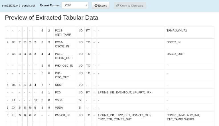
Tabula has a nice local web interface which gives you previews of the table data that it will export from a PDF.
Step 1: Download Tabula
Tabula runs on Java, so it’s simple to set up on just about any platform. They have good installation instructions on their website and GitHub readme file. If you are using Linux, you can download and unzip the tabula-jar-<version>.zip version of the latest release to get a runnable JAR file.
Following the instructions in the README.md file, once you unzip the file and cd into its tabula/ directory, you can start running a local server with the command that the readme file suggests:
java -Dfile.encoding=utf-8 -Xms256M -Xmx1024M -jar tabula.jar
Once it starts up, you should be able to navigate to http://127.0.0.1:8080 in a browser to access the Tabula UI. There is also a command-line version of the project, which will probably be better for setting up an automatic process. But for now, it’s nice to use the visual selection tools which the UI provides.
Making Pretty(ish) Reference Images for Microcontrollers
When you want to pick a microcontroller for a project, it can be useful to have a bunch of quick references to find the smallest/cheapest one that will fit the parts you want to use. Usually the information is freely available in datasheets, but those are usually PDF files with pinout/peripheral information spanning several pages.
So I’ve been playing with ways to partially automate the process of generating some nice reference images. I’m not exactly happy with what I have yet, but it’s not the sort of thing that merits spending a ton of time on, and I think I scripted away enough of the tedium that it isn’t too frustrating to make these sorts of tables. You wind up with reference images like this:
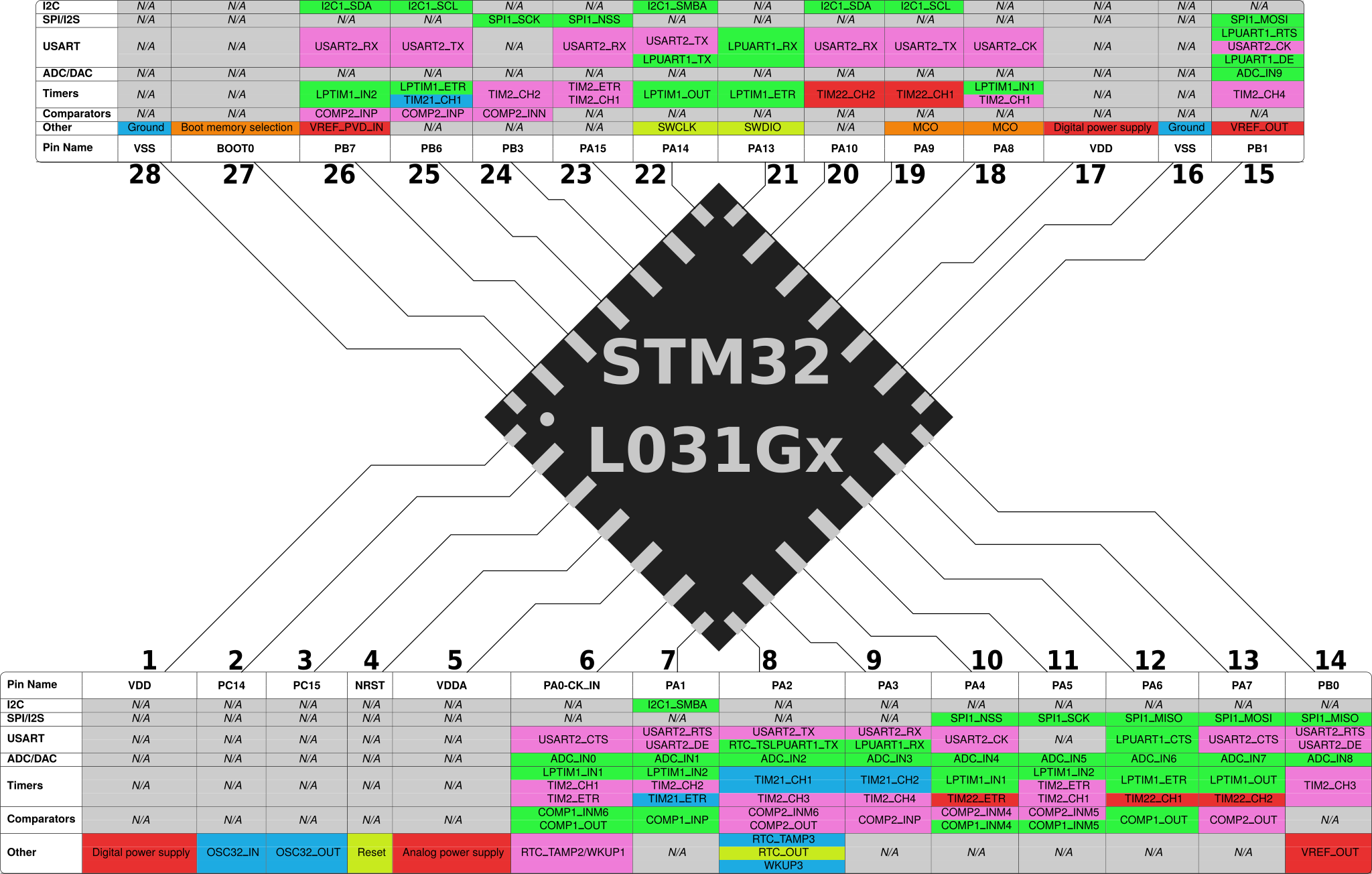
STM32L031Gx Pinout / Peripherals
Honestly, this post would be sort of moot if I could find nice CSV files or spreadsheets of STM32 pinouts and peripherals (see below). Maybe other vendors distribute information in that format, but I couldn’t find many for ST’s chips. And that means that I ended up with a sort of convoluted process.
A fragile Python script runs the pdftotext utility to convert an STM32 datasheet into a pinout table containing peripheral information. The automatic formatting doesn’t include table cell boundaries, so I couldn’t figure out how to put all of the peripherals associated with a pin on the same line quickly; someone needs to manually perform that step before running a second Python script which generates LaTeX files representing formatted peripheral tables. The PDF files generated by pdflatex can then be imported into Inkscape, where the table columns can be connected to the pins on an image of the chip’s outline. So, let’s get started!
Note: I ended up finding a better way to parse STM32 datasheets using a project called Tabula – see this newer post for more information. My first attempt presented in this post ended up working pretty poorly, but that’s life for you. Sometimes it takes a few tries to find a good solution.
Getting Started with Bare Metal ESP32 Programming
The ESP32 modules sold by Espressif are very popular in the IoT and embedded development space. They are very cheap, they are quite fast, they include radios and peripherals for WiFi and Bluetooth communication, and in some ways they even appear to bridge the gap between MCU and CPU. And Espressif provides pre-built modules with built-in antennas and external Flash memory, both of which appear to be required for general-purpose ‘IoT’ application development. They can be a bit power-hungry when they are using their wireless communication modules though, and I haven’t found much information on how to develop ESP32 applications without using the heavyweight (but very functional and well-written) “ESP-IDF” toolchain which is distributed by Espressif.
Usually, avoiding bulky and proprietary HALs is a worthwhile goal in and of itself. But Espressif has actually released their ESP-IDF toolchain under a very permissive Apache license, and it looks like a well-thought-out system with solid ongoing support. So if you are looking at starting a new project with the ESP32, I would personally recommend using the ESP-IDF to save time and effort. But sometimes it is nice to learn about how chips work at a deeper level, and ESP-IDF projects are often quite large, and they can take a long time to build depending on your environment.
The large code size also discourages what appears to be one use case that the chip was designed for: to load new instructions into RAM every time that it reboots from an external ‘socket’. The current crop of ESP32 modules use a SPI Flash chip as that ‘socket’, but if you put them in a factory or a field you might want to use Ethernet, or RS-232, or who knows what. I’m not sure how extensible the chip’s ROM bootloader actually is yet, but let’s take a look at what it takes to get a simple C program running on the ESP32 without using the ESP-IDF build system.
Unlike the STM32 and MSP430 microcontrollers which I have written about previously, there are not many software tools available for the ESP32 core. The ESP32’s dual-core architecture uses two ‘Xtensa LX6’ CPU cores which Espressif licenses from Cadence, and I haven’t seen them in any other mainstream microcontrollers. It looks like a core that is intended to be customized for the needs of an application as a step between general-purpose microcontrollers and something like an ASIC, so maybe it is more common in application-specific environments than general-purpose ones. In this case, it looks like the specific application which Espressif chose is wireless communication, and apparently a lot of the WiFi and Bluetooth code is burned directly into the ESP32’s ROM.
The ESP32 also looks more like a proper CPU than many microcontroller cores, with a few hundred kilobytes of on-chip RAM, a 240MHz top speed, an MMU, and support for up to 8 process IDs (2 privileged / 6 unprivileged) per core. People used to make do with much less, but since the ESP32 is complex and somewhat unique, Espressif provides the only toolchain that I know about which can build code for it. That means that while this tutorial will not use the full ESP-IDF development environment, it will still use Espressif’s ports of GCC and OpenOCD for compilation and debugging, as well as their esptool utility for formatting and flashing the compiled code. The target hardware will be either the ESP32-WROVER-KIT board which includes a JTAG debugging chip, or any of the smaller generic ESP32 dev boards (such as the ESP32-DevKitC) combined with an FTDI C232HM cable.
And like most of my previous tutorials, the software presented here is all open-source and you should be able to build and run it on the platform of your choice. It won’t have any colorful LEDs this time – sorry – but the code is available on GitHub. I’m also still learning about this chip and there is a lot that I don’t know, so corrections and comments are definitely appreciated. So if you’re still interested after those disclaimers, let’s get started by building and installing the toolchain!
Building a Bare-Metal ARM GCC Toolchain from Source
The GCC toolchain is a nice way to get started with bare-metal ARM platforms because it is free, well-supported, and something that many C programmers are already familiar with. It is also constantly improving, and while most Linux distributions include a version of the arm-none-eabi GCC toolchain in their default package managers, those versions are sometimes old enough that I run into bugs with things like multilib/multiarch support.
So after trying and failing a few times to build and install this toolchain, I thought I would share what eventually worked for me. If you are building this on a system without much free disk space, this did take about 16GB of disk space when I ran it – but you shouldn’t need to keep more than ~500MB of that. I ended up building it on an ext3-formatted 32GB USB drive, and that seemed to work fine. You will probably run into errors if you try to run this on a FAT-formatted drive like a new USB stick, though, because the build process will run chmod and that will fail on a filesystem that doesn’t support file permissions. You might be able to make it work with an NTFS drive, but I digress.
Anyways, the first step is downloading the code, so let’s get started!
Step 1: Download the Source Code
The first step is to download the arm-none-eabi-gcc source code from ARM’s website – you want the “Source Invariant” version. If you are using a common architecture such as x86_64, you can also download a pre-built version of the latest release, but you probably want to build the thing yourself if you are reading this guide. If you want to make sure that the file you downloaded was not corrupted or tampered with, you can check it against the MD5 checksum listed under the file’s name on the download page:
> md5sum gcc-arm-none-eabi-8-2018-q4-major-src.tar.bz2
d6071d95064819d546fe06c49fb9d481 gcc-arm-none-eabi-8-2018-q4-major-src.tar.bz2
That looks like it matches as of the time of writing. The archive contains build scripts and code for the whole toolchain, so create a new directory to build the toolchain in – I’ll use ~/arm_gcc/ as an example. Once it finishes downloading, move the archive to that folder and extract it:
> mkdir ~/arm_gcc
> cd ~/arm_gcc
> mv [Your_Downloads_Folder]/gcc-arm-none-eabi-8-2018-q4-major-src.tar.bz2 .
> tar -xvf gcc-arm-none-eabi-8-2018-q4-major-src.tar.bz2
The file that I downloaded was called gcc-arm-none-eabi-8-2018-q4-major-src.tar.bz2, but yours will depend on where you are in time. The extracted archive will make a new directory with a similar name – take a look inside, and you’ll see a few scripts and a ‘how-to’ document alongside the source code:
> cd gcc-arm-none-eabi-8-2018-q4-major/
> ls
build-common.sh build-toolchain.sh install-sources.sh python-config.sh release.txt
build-prerequisites.sh How-to-build-toolchain.pdf license.txt readme.txt src
Keeping Up With the Moorses: Learning to Use STM32G0 Chips
Microcontrollers are just like any other kind of semiconductor product. As manufacturers learn from customer feedback and fabrication processes continue to advance, the products get better. One of the most visible metrics for gauging a chip’s general performance – and the basis of Moore’s Law – is how large each transistor is. Usually this is measured in nanometers, and as we enter 2019 the newest chips being made by companies like Samsung and Intel are optimistically billed as 7nm.
The venerable and popular STM32F1 series is more than a decade old now, and it is produced using a 130nm process. But ST’s newer lines of chips like the STM32L4 use a smaller 90nm process. Smaller transistors usually mean that chips can run at lower voltages, be more power-efficient, and run at faster clock speeds. So when ST moved to this smaller process, they introduced two types of new chips: faster ‘mainline’ chips like the F4 and F7 lines which run at about 100-250MHz, and more efficient ‘low-power’ chips like the L0 and L4 lines which have a variety of ‘sleep’ modes and can comfortably run off of 1.8V. They also have an H7 line which uses an even smaller 40nm process and can run at 400MHz.
Now as 2018 fades into history, it looks like ST has decided that it’s time for a fresh line of ‘value-line’ chips, and we can order a shiny new STM32G0 from retailers like Digikey. At the time of writing there aren’t too many options, but it looks like they’re hoping to branch out and there are even some 8-pin variants on the table. I could be misreading things, but these look like a mix between the F0 and L0 lines, with lower power consumption than F0 chips and better performance than the L0 chips. The STM32G071GB that I made a test board with has 128KB of Flash, 36KB of RAM, and a nice set of communication peripherals.
Simple STM32G0 breakout board
So what’s the catch? Well, this is still a fairly new chip, so “Just Google It” may not be an effective problem-solving tool. And it looks like ST made a few changes in this new iteration of chips to provide more GPIO pins in smaller packages, so the hardware design will look similar but slightly different from previous STM32 lines. Finally, with a new chip comes new challenges in getting an open-source programming and debugging toolchain working. So with all of that said, let’s learn how to migrate!
“Bare Metal” STM32 Programming (Part 8): Learn to Debug Timing Issues with Neopixels
I haven’t written about STM32 chips in a little while, but I have been learning how to make fun displays and signage using colorful LEDs, specifically the WS2812B and SK6812 ‘Neopixels’. I talked about the single-wire communication standard that these LEDs use in a post about running them from an FPGA, and I mentioned there that it is a bit more difficult for microcontrollers to run the communication standard. If you don’t believe me, take a look at what the poor folks at Adafruit needed to do to get it working on a 16MHz AVR core. Yikes!
When you send colors, the 1 bits are fairly easy to encode but the 0 bits require that you reliably hold a pin high for just 250-400 nanoseconds. Too short and the LED will think that your 0 bit was a blip of noise, too long and it will think that your 0 is a 1. Using timer peripherals is a reasonable solution, but it requires a faster clock than 16MHz and we won’t be able to use interrupts because it takes about 20-30 clock cycles for the STM32 to jump to an interrupt handler. At 72MHz it takes my code about 300-400 nanoseconds to get to an interrupt handler, and that’s just not fast enough.
There are ways to make it faster, but this is also a good example of how difficult it can be to calculate how long your C code will take to execute ahead of time. Between compiler optimizations and hardware realities like Flash wait-states and pushing/popping functions, the easiest way to tell how long your code takes to run is often to simply run it and check.
Pulseview diagram of ‘101’ in Neopixel. I can’t be sure, but I think the ‘0’ pulse might be about 375 nanoseconds long.
Which brings us to the topic of this tutorial – we are going to write a simple program which uses an STM32 timer peripheral to draw colors to ‘Neopixel’ LEDs. Along the way, we will debug the program’s timing using Sigrok and Pulseview with an affordable 8-channel digital logic analyzer. These are available for $10-20 from most online retailers; try Sparkfun, or Amazon/eBay/Aliexpress/etc. I don’t know why Adafruit doesn’t sell these; maybe they don’t want to carry cheap generics in the same category as Salae analyzers. Anyways, go ahead and install Pulseview, brush up a bit on STM32 timers if you need to, and let’s get started!
Learning how to FPGA with ‘Neopixel’ LEDs
Whenever I talk to someone about FPGAs, the conversation seems to follow a familiar routine. It is almost a catechism to say that ‘FPGAs are very interesting niche products that, sadly, rarely make sense in real-world applications’. I often hear that organizations with Money can afford to develop ASICs, while hobbyists are usually better served by today’s affordable and powerful microcontrollers except in some very specific circumstances like emulating old CPU architectures. I don’t have enough experience to know how accurate this is, but I do have a couple of projects that seem like they could benefit from an FPGA, so I decided to bite the bullet and learn the basics of how to use one.
I chose a popular $25 development board called the ‘Icestick‘ to start with. It uses one of Lattice’s iCE40 chips, which is nice because there is an open-source toolchain called Icestorm available for building Verilog or VHDL code into an iCE40 bitstream. Most FPGA vendors (including Lattice) don’t provide a toolchain that you can build from source, but thanks to the hard work of Clifford Wolf and the other Icestorm contributors, I can’t use “maddeningly proprietary tools” as a reason not to learn about this anymore.
One thing that FPGAs can do much better than microcontrollers is running a lot of similar state machines in parallel. I’d eventually like to make a ‘video wall’ project using individually-addressable LEDs, but the common ‘Neopixel’ variants share a maximum data rate of about 800kbps. That’s probably too slow to send video to a display one pixel at a time, but it might be fast enough to send a few hundred ‘blocks’ of pixel data in parallel. As a small step towards that goal, I decided to try lighting up a single strip of WS2812B or SK6812 LEDs using Verilog. Here, I will try to describe what I learned.
Blue Icestick
And while this post will walk through a working design, I’m sorry that it will not be a great tutorial on writing Verilog or VHDL; I will try to gloss over what I don’t understand, so I would encourage you to read a more comprehensive tutorial on the subject like Al Williams’ series of Verilog and Icestorm tutorials on Hackaday. Sorry about that, but I’m still learning and I don’t want to present misleading information. This tutorial’s code is available on Github as usual, but caveat emptor.
Basic MSP430 Hardware Design
Evaluation boards are great, but eventually you’ll want to make a design which needs to fit in a smaller space, or which uses a type of chip that doesn’t have a cheap board available. When that happens, you’ll often want to design a PCB. And it seems like most microcontrollers have similar basic hardware requirements; decoupling capacitors on the power pins, maybe a pull-up resistor and filtering capacitor on the reset pin, and a few pins which are used for debugging and programming. The MSP430 is no different, although it does have a few small quirks to be aware of.
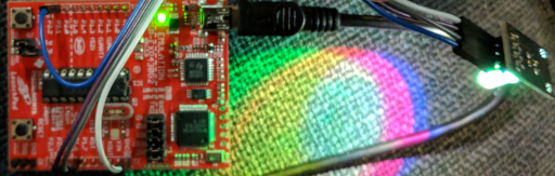
And while I haven’t found a cheap dedicated USB device for programming MSP430 chips, you can use the debuggers built into TI’s Launchpad boards to program and debug a custom board using their “Spy-Bi-Wire” protocol. So in this tutorial, I’ll go over a basic circuit design for an MSP430FR2111 chip. It comes in a TSSOP-16 package with 3.75KB of FRAM and no Flash memory.
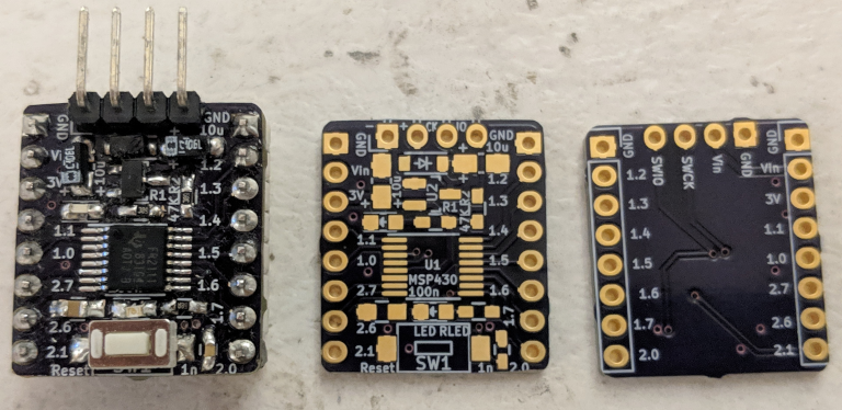
A simple example MSP430FR2111 breakout board design.
I’ll also go over the differences between programming a ‘pulsing LED’ example for the MSP430FR2111 and the MSP430G2553 that we used in the last two examples, as well as how to connect a Launchpad board’s debugger to upload programs to the custom board. So let’s get started!
Basic Low-Power Design: Sleepy PWM on the MSP430
Recently, I wrote about setting up a basic ‘hello, world’ program for an MSP430 microcontroller. These chips look like they are designed to make low-power designs easy to code, so it seems like a good idea to start learning about their low-power sleep modes. TI claims that, at 3V and a 1MHz core clock speed, an MSP430x2xx will consume about 300μA while running, 55μA in “low-power mode 0”, and as little as 0.1μA in “low-power mode 4”. But you may have difficulty reaching those figures on a Launchpad board because of how the circuit is laid out.
You can see section 2.3 of the reference manual for more details on these sleep modes, but the most important thing to know is that different low-power modes can selectively disable the core CPU, system clocks, and peripherals on the chip. Some clocks and peripherals remain active in some low-power modes. For example, the chip’s timers can continue to run while the CPU is off as long as the system clock they are connected to is still active.
So in this tutorial, we’ll walk through pulsing a common-cathode RGB LED through various colors using the MSP430’s timers to generate PWM signals while the chip rests in LPM0 sleep mode. We need to set up the timers and attach an interrupt to periodically change the PWM duty cycles, but once that is done we can turn off the CPU. The timer interrupt will periodically wake it up, and the chip will automatically go back to sleep after the interrupt handler returns.
“Common-Cathode” LEDs let you control a red, green, and blue LED individually using PWM signals. Each LED is connected to the same cathode (‘ground’).
This post’s Github repository contains two projects; one which dims and brightens a single on-board LED using PWM, and one which uses a timer interrupt to pulse each color in a common-cathode RGB LED while putting the device to sleep when it is not active.
“Bare Metal” MSP430 Programming: Learning About a New Microcontroller
Most of the embedded programming that I’ve written about so far has focused on the STM32 family of ARM microcontrollers produced by ST Microelectronics. Those are a reasonable starting point for learning about microcontrollers, because they have a solid suite of open-source development tools, a decade-long history of popular use, and affordable hardware development tools which let you get started for less than $20.
But now that platforms like Arduino have become popular and presumably profitable, more vendors are getting on board with providing affordable “DIY” development tools. So while I couldn’t find any cheap and widely-available USB debuggers for TI’s MSP430 core, the “Launchpad” boards that they sell each include an on-board debugger which they say can talk to most MSP430 chips through a two-wire interface similar to the “Serial-Wire Debug” protocol used by a number of Mobile ARM cores including the STM32.
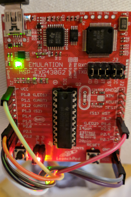
Like the Arduino Uno, some Launchpad boards use DIP chips which you can remove and plug into a breadboard once they have been programmed.
So let’s learn how to write bare-metal programs for the MSP430! This will be easier than bootstrapping a build system for the STM32, because TI opted to design a special-purpose 16-bit RISC core for these chips instead of buying a cookie-cutter core from ARM. That means that the MSP430-GCC toolchain can include ‘glue’ code like linker scripts and vector tables for every MSP430 chip ever made, and we will not need to write our own. There are also fewer steps involved in setting up clocks and peripherals, so this is a comparatively easy platform to develop on. And as usual, this tutorial’s code is on Github.