
Talking to Hardware
“Bare Metal” STM32 Programming (Part 12): Using Quad-SPI Flash Memory
If I had to guess what the world’s most popular footprint for low-density memory chips was, I would probably be wrong. But I’ll bet that the humble 8-pin SOIC / DIP / DFN formats would be near the top. You’ve probably used these before; most ESP8266 and ESP32 modules have one under their little metal shield, and motherboards for computers / cars / synthesizers / etc. often use them for storing UEFI / BIOS / firmware configurations and suchlike.
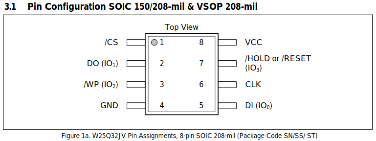
Pin assignments for a generic Flash module (Winbond W25Q series)
You can get RAM, Flash, EEPROM, and even FRAM memory in these common 8-pin packages. They usually use a SPI interface for communication, with a couple of extra pins for functions like write protection or suspending an ongoing transaction. But if you look in the image above, you’ll see that the /WP “Write Protect” and /HOLD or /RESET wires are also marked as IO2 and IO3. That’s because many 8-pin Flash chips also support a “Quad-SPI” interface, which is very similar to a bidirectional “3-wire” SPI interface, except that it has four I/O wires instead of one.
Some STM32 chips include a QSPI peripheral to interface with these kinds of Flash memory chips. You can use it to manually configure / erase / program the Flash chip, and once it’s initialized, you can also map the external Flash as read-only memory in the STM32’s internal memory space. The peripheral supports prefetching, caching, executing code, and it can even access two QSPI Flash chips in parallel, using 8 data lines in total to transfer a full byte of data every clock cycle.
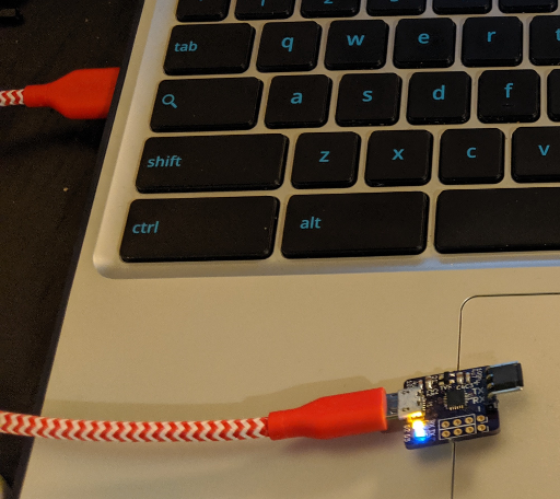
To learn about the QSPI peripheral, I used the same STM32F723E Discovery Kit from my last post about external memories. In addition to its external RAM and display, this board includes one 64MB QSPI Flash chip connected to the QSPI peripheral. In this post, we’ll learn how to configure the Flash chip for quad I/O access, erase a sector, and write some test values. Then we’ll set the QSPI peripheral to its read-only “memory-mapped” mode, and read those test values by accessing the chip’s internal memory space starting at 0x90000000. If you don’t like copy/pasting, you can find an example project with this code on GitHub.
It is a little bit annoying that you can’t write to the Flash chip in memory-mapped mode, but this peripheral still presents a simple way to quickly read from external Flash using only six I/O pins. And writing to Flash memory has some unique limitations anyways, which is why it is often used to store data which an application rarely needs to modify, like firmware or audio/visual resources. So if you want to learn how to use Quad-SPI Flash memories with an STM32, read on!
“Bare Metal” STM32 Programming (Part 11): Using External Memories
Modern microcontrollers are amazing. They are much faster and cheaper than the sort of processors that powered “real” computers a few decades ago, and they’re also very power-efficient. But software complexity has also grown over time, and as we humans often say about ourselves as we age, it has grown in the wrong direction. Developers have gotten used to having enormous reserves of memory to draw from, so unless an application or library was specifically written for embedded platforms, it probably won’t be able to run with the scant kilobytes of RAM which are included in your average microcontroller.
Fortunately, most vendors include peripherals for accessing external memory when it is needed, and the STM32’s “Flexible Memory Controller” is surprisingly easy to use. Unfortunately, it is not easy to design a custom PCB with parallel memory modules. The interfaces use a lot of signals which are susceptible to electromagnetic noise, so it is important to ensure that all of the traces have the same length and impedance. This is especially hard on hobbyists, because 2-layer boards are not appropriate for these sorts of designs and KiCAD does not support length-matching for more than two traces yet.
So the target hardware for this tutorial will be a $40 STM32F723E Discovery Kit. It is a bit more expensive than the minimal “Nucleo” boards, but it includes 512KB of external RAM and a 240×240-pixel TFT display; we’ll learn how to drive both of those from the FMC peripheral in this post. It also includes 64MB of memory-mapped QSPI Flash memory, which I’ll talk about in a future post.
We’ll use the external RAM to store a framebuffer, which will be sent to the display using DMA.
This evaluation board uses BGA parts, which are almost impossible to solder without special equipment. But it provides an easy and affordable way to learn about writing software for these peripherals. When you are ready to use external memories in homemade designs, you can use QFP STM32s with at least 144 pins, TSSOP memory chips, and a 4-layer PCB.
Learning FPGA Design with nMigen
Like many of us, I’ve been stuck indoors without much to do for the past month or so. Unfortunately, I’m also in the process of moving, so I don’t know anyone in the local area and most of my ‘maker’ equipment is in storage. But there’s not much point in sulking for N months straight, so I’ve been looking at this as an opportunity to learn about designing and implementing FPGA circuits.
I tried getting into Verilog a little while ago, but that didn’t go too well. I did manage to write a simple WS2812B “NeoPixel” driver, but it was clunky and I got bored soon after. In my defense, Verilog and VHDL are not exactly user-friendly or easy to learn. They can do amazing things in the hands of people who know how to use them, but they also have a steep learning curve.
Luckily for us novices, open-source FPGA development tools have advanced in leaps and bounds over the past few years. The yosys and nextpnr projects have provided free and (mostly) vendor-agnostic tools to build designs for real hardware. And a handful of high-level code generators have also emerged to do the heavy lifting of generating Verilog or VHDL code from more user-friendly languages. Examples of those include the SpinalHDL Scala libraries, and the nMigen Python libraries which I’ll be talking about in this post.
I’ve been using nMigen to write a simple RISC-V microcontroller over the past couple of months, mostly as a learning exercise. But I also like the idea of using an open-source MCU for smaller projects where I would currently use something like an STM32 or MSP430. And most importantly, I really want some dedicated peripherals for driving cheap addressable “NeoPixel” LEDs; I’m tired of needing to mis-use a SPI peripheral or write carefully-timed assembly code which cannot run while interrupts are active.
But that will have to wait for a follow-up post; for now, I’m going to talk about some simpler tasks to introduce nMigen. In this post, we will learn how to read “program data” from the SPI Flash chip on an iCE40 FPGA board, and how to use that data to light up the on-board LEDs in programmable patterns.
The LEDs on these boards are very bright, because you’re supposed to use PWM to drive them.
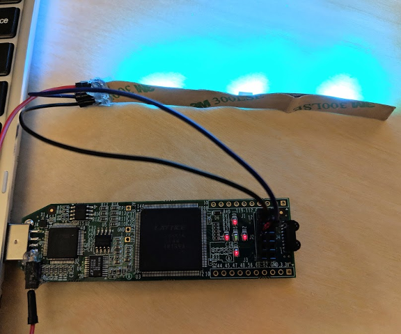
The target hardware will be an iCE40UP5K-SG48 chip, but nMigen is cross-platform so it should be easy to adapt this code for other FPGAs. If you want to follow along, you can find a 48-pin iCE40UP5K on an $8-20 “Upduino” board or a $50 Lattice evaluation board. If you get an “Upduino”, be careful not to mis-configure the SPI Flash pins; theoretically, you could effectively brick the board if you made it impossible to communicate with the Flash chip. The Lattice evaluation board has jumpers which you could unplug to recover if that happens, but I don’t think that the code presented here should cause those sorts of problems. I haven’t managed to brick anything yet, knock on wood…
Be aware that the Upduino v1 board is cheaper because it does not include the FT2232 USB/SPI chip which the toolchain expects to communicate with, so if you decide to use that option, you’ll need to know how to manually write a binary file to SPI Flash in lieu of the iceprog commands listed later in this post.
Designing a Simple GPS Handheld
I’ve written a little bit in the past about how to design a basic STM32 breakout board, and how to write simple software that runs on these kinds of microcontrollers. But let’s be honest: there’s still a bit of a gap between creating a small breakout board to blink an LED, and building hardware / software for a ‘real-world’ application. Personally, I would still want a couple of more experienced engineers to double-check any designs that I wanted to be reliable enough for other people to use, but building more complex applications is a great way to help yourself learn.
So in this post, I’m going to walk through the process of designing a small ‘gameboy’-style handheld with a GPS receiver and microSD card slot, for exploring the outdoors instead of video games. Don’t get me wrong, you could still write games to run on this if you wanted to, and that would be fun, but everyone and their dog has made a Cortex-M-based handheld game console by now; there are plenty of better guides for that, and many of those authors put a lot more time into their designs and firmware than I ever did.
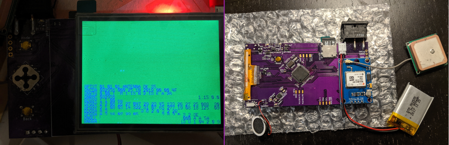
Assembled GPS Doohicky. I left too much room between the ribbon connector footprint and the edge of the board on this first revision, so the display couldn’t fold over quite right. Oh well, you live and learn.
The board design isn’t too complicated, but there are several different parts and it gets easier to make small-but-important mistakes as a design gets larger. It mostly uses peripherals that I’ve talked about previously, but there are a couple of new ones too. The display will be driven over SPI, the speaker uses a DAC, the GPS receiver talks over UART, the battery and light levels will be read using an ADC, and the buttons will be listened to using interrupts. But I haven’t written about the USB or SD card (“MMC”) peripherals, and those will need to go in a future post since I haven’t actually worked them out myself yet. Note that SD cards can technically use either SPI or SD/MMC to communicate, but the microcontroller that I picked has a dedicated SD/MMC peripheral, and I wanted to learn about it.
Anyways, if that sounds interesting, read on and let’s get started!
Simple USB / Serial Communication with the CP2102N
Several years ago, a company called Future Technology Devices International (FTDI) sold what may have been the most popular USB / Serial converter on the market at the time, called the FT232R. But this post is not about the FT232R, because that chip is now known for its sordid history. Year after year, FTDI enjoyed their successful chip’s market position – some would say that they rested too long on their laurels without innovating or reducing prices. Eventually, small microcontrollers advanced to the point where it was possible to program a cheap MCU to identify itself as an FT232R chip and do the same work, so a number of manufacturers with questionable ethics did just that. FTDI took issue with the blatant counterfeiting, but they were unable to resolve their dispute through the legal system to their satisfaction, possibly because most of the counterfeiters were overseas and difficult to definitively trace down. Eventually, they had the bright idea of publishing a driver update which caused the counterfeit chips to stop working when they were plugged into a machine with the newest drivers.
FTDI may have technically been within their rights to do that, but it turned out to be a mistake as far as the market was concerned – as a business case study, this shows why you should not target your customers in retaliation for the actions of a 3rd party. Not many of FTDI’s customers were aware that they had counterfeit chips in their supply lines – many companies don’t even do their own purchasing of individual components – so companies around the world started to get unexpected angry calls from customers whose toy/media device/etc mysteriously stopped working after being plugged into a Windows machine. You might say that this (and the ensuing returns) left a bad taste in their mouths, so while FTDI has since recanted, a large vacuum opened up in the USB / Serial converter market almost overnight.
Okay, that might be a bit of a dramatized and biased take, but I don’t like it when companies abuse their market positions. Chips like the CH340 and CH330 were already entering the low end of the market with ultra-affordable and easy-to-assemble solutions, but I haven’t seen them much outside of Chinese boards, possibly due to a lack of multilingual documentation or availability from Western distributors. So at least in the US, the most popular successor to the FT232R seems to have been Silicon Labs’ CP2102N.
It’s nice to have a cheap-and-cheerful way to put a USB plug which speaks UART onto your microcontroller boards, so in this post, I’ll review how to make a simple USB / UART converter using the CP2102N. The chip comes in 20-, 24-, and 28-pin variants – I’ll use the 24-pin one because it’s smaller than the 28-pin one and the 20-pin one looks like it has some weird corner pads that might be hard to solder. We’ll end up with a simple, small board that you can plug into a USB port to talk UART:
Drivers for the CP2102N are included in most popular OSes these days, including Linux distributions, so it’s mostly plug-and-play.
It’s worth noting that you can buy minimal CP2102N boards from AliExpress or TaoBao for about $1, but where’s the fun in that?
“Bare Metal” STM32 Programming (Part 8): Learn to Debug Timing Issues with Neopixels
I haven’t written about STM32 chips in a little while, but I have been learning how to make fun displays and signage using colorful LEDs, specifically the WS2812B and SK6812 ‘Neopixels’. I talked about the single-wire communication standard that these LEDs use in a post about running them from an FPGA, and I mentioned there that it is a bit more difficult for microcontrollers to run the communication standard. If you don’t believe me, take a look at what the poor folks at Adafruit needed to do to get it working on a 16MHz AVR core. Yikes!
When you send colors, the 1 bits are fairly easy to encode but the 0 bits require that you reliably hold a pin high for just 250-400 nanoseconds. Too short and the LED will think that your 0 bit was a blip of noise, too long and it will think that your 0 is a 1. Using timer peripherals is a reasonable solution, but it requires a faster clock than 16MHz and we won’t be able to use interrupts because it takes about 20-30 clock cycles for the STM32 to jump to an interrupt handler. At 72MHz it takes my code about 300-400 nanoseconds to get to an interrupt handler, and that’s just not fast enough.
There are ways to make it faster, but this is also a good example of how difficult it can be to calculate how long your C code will take to execute ahead of time. Between compiler optimizations and hardware realities like Flash wait-states and pushing/popping functions, the easiest way to tell how long your code takes to run is often to simply run it and check.
Pulseview diagram of ‘101’ in Neopixel. I can’t be sure, but I think the ‘0’ pulse might be about 375 nanoseconds long.
Which brings us to the topic of this tutorial – we are going to write a simple program which uses an STM32 timer peripheral to draw colors to ‘Neopixel’ LEDs. Along the way, we will debug the program’s timing using Sigrok and Pulseview with an affordable 8-channel digital logic analyzer. These are available for $10-20 from most online retailers; try Sparkfun, or Amazon/eBay/Aliexpress/etc. I don’t know why Adafruit doesn’t sell these; maybe they don’t want to carry cheap generics in the same category as Salae analyzers. Anyways, go ahead and install Pulseview, brush up a bit on STM32 timers if you need to, and let’s get started!
Learning how to FPGA with ‘Neopixel’ LEDs
Whenever I talk to someone about FPGAs, the conversation seems to follow a familiar routine. It is almost a catechism to say that ‘FPGAs are very interesting niche products that, sadly, rarely make sense in real-world applications’. I often hear that organizations with Money can afford to develop ASICs, while hobbyists are usually better served by today’s affordable and powerful microcontrollers except in some very specific circumstances like emulating old CPU architectures. I don’t have enough experience to know how accurate this is, but I do have a couple of projects that seem like they could benefit from an FPGA, so I decided to bite the bullet and learn the basics of how to use one.
I chose a popular $25 development board called the ‘Icestick‘ to start with. It uses one of Lattice’s iCE40 chips, which is nice because there is an open-source toolchain called Icestorm available for building Verilog or VHDL code into an iCE40 bitstream. Most FPGA vendors (including Lattice) don’t provide a toolchain that you can build from source, but thanks to the hard work of Clifford Wolf and the other Icestorm contributors, I can’t use “maddeningly proprietary tools” as a reason not to learn about this anymore.
One thing that FPGAs can do much better than microcontrollers is running a lot of similar state machines in parallel. I’d eventually like to make a ‘video wall’ project using individually-addressable LEDs, but the common ‘Neopixel’ variants share a maximum data rate of about 800kbps. That’s probably too slow to send video to a display one pixel at a time, but it might be fast enough to send a few hundred ‘blocks’ of pixel data in parallel. As a small step towards that goal, I decided to try lighting up a single strip of WS2812B or SK6812 LEDs using Verilog. Here, I will try to describe what I learned.
Blue Icestick
And while this post will walk through a working design, I’m sorry that it will not be a great tutorial on writing Verilog or VHDL; I will try to gloss over what I don’t understand, so I would encourage you to read a more comprehensive tutorial on the subject like Al Williams’ series of Verilog and Icestorm tutorials on Hackaday. Sorry about that, but I’m still learning and I don’t want to present misleading information. This tutorial’s code is available on Github as usual, but caveat emptor.
More Fun with Four-Wire SPI: Drawing to “E-Ink” Displays
In previous tutorials, I covered how to use the STM32 line of microcontrollers to draw to small displays using the SPI communication standard. First with software functions and small ‘SSD1331’ OLED displays, and then with the faster SPI hardware peripheral and slightly larger ‘ILI9341’ TFT LCD displays. Both of those displays are great for cheaply displaying data or multimedia content, because they can show 16 bits of color per pixel and have enough space to present a moderate amount of information. But if you want to design a very low-power application, you might want a display which does not need to constantly drain energy to maintain an image.
Enter ‘E-Ink’ displays, sometimes called “Electrophoretic Displays“. As the name implies, they use the same basic operating principle as techniques like Gel Electrophoresis, which separates polarized molecules such as DNA based on their electric charge. Each pixel in one of these displays is a tiny hollow sphere filled with oppositely-charged ink molecules, and they are separated between the top and bottom of their capsules to make the pixel light or dark. The ink remains in place even after power is removed; I think that they are suspended in a solid gel or something. Modern E-Ink modules sometimes have a third color such as red or yellow, but this post will only cover a humble monochrome display.
E-ink 😀
Drawing to a Small TFT Display: the ILI9341 and STM32
As you learn about more of your microcontroller’s peripherals and start to work with more types of sensors and actuators, you will probably want to add small displays to your projects. Previously, I wrote about creating a simple program to draw data to an SSD1331 OLED display, but while they look great, the small size and low resolution can be limiting. Fortunately, the larger (and slightly cheaper) ILI9341 TFT display module uses a nearly-identical SPI communication protocol, so this tutorial will build on that previous post by going over how to draw to a 2.2″ ILI9341 module using the STM32’s hardware SPI peripheral.
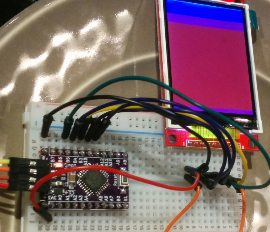
An ILI9341 display being driven by an STM32F0 chip. Technically this isn’t a ‘Nucleo’ board, but the code is the same.
We’ll cover the basic steps of setting up the required GPIO pins, initializing the SPI peripheral, starting the display, and then finally drawing pixel colors to it. This tutorial won’t read any data from the display, so we can use the hardware peripheral’s MISO pin for other purposes and leave the TFT’s MISO pin disconnected. And as with my previous STM32 posts, example code will be provided for both the STM32F031K6 and STM32L031K6 ‘Nucleo’ boards.
When is Now? The DS3231 Real-Time Clock
Time may be an artificial construct, but try telling your boss that ‘Monday’ has no meaning. It is useful for a program to be able to schedule actions for a certain date, display the current time on a clock or calendar, or perform other tasks which use weird units of time like ‘seconds’ or ‘days’. For those types of tasks, an embedded developer might reach for an ‘RTC’ device, which stands for ‘Real-Time Clock’. They provide a way to keep accurate time, often with features like backup power supplies. Many RTCs also offer ‘wakeup’ alarms for other devices, so they are especially useful in energy-efficient designs.
The STM32 line of chips which I’ll continue to use in this tutorial have a built-in RTC peripheral, but they require an external 32.768KHz ‘LSE’ (Low-Speed External) crystal oscillator to keep accurate time. Also, managing the STM32’s backup power supply is sort of complicated.
Instead, this tutorial will walk through using the ‘I2C’ peripheral on an STM32 chip to communicate with a cheap DS3231 RTC module. Specifically, I will talk about a widely-available board labeled ZS-042, which includes 4KB of EEPROM on its I2C bus and space for a “coin cell” battery to provide several years of backup power. But the same commands should work with other DS3231 boards, such as the smaller ones in the upper-left here:
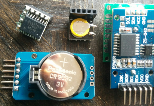
A handful of DS3231 modules and their backup batteries.
An example project demonstrating the concepts outlined in this post using either an STM32F031K6 or STM32L031K6 “Nucleo” board is available on Github.