
For the past few years, there has been growing excitement about the RISC-V instruction set architecture. It is an appealing architecture because it is open-source (which can mean royalty-free), and flexible enough to be configured for everything from small power-efficient microcontrollers to fast and complex application processors. In this post, we’ll learn how to write a simple program for a GigaDevice GD32VF103 chip, which leans towards the “small and power-efficient” end of the spectrum.
There have already been a handful of opportunities for hobbyists to use RISC-V hardware in their projects, such as the SiFive “Freedom” chips and Kendryte K210 modules. But the SiFive boards are expensive and (up until this point) produced in limited quantities, and most of the cheaper options have been narrowly focused on niches like machine learning or IoT applications. The GD32VF103 is still fairly new, and while there’s no guarantee that it won’t end up in history’s dustbin of one-off chips, it is an affordable general-purpose chip with a few tricks up its sleeve which should make it a nice learning platform.
First, it is easy to buy a handful of boards which use these chips: you can buy “Longan Nano” boards for about $5 from Seeed Studios, and they also sell compatible USB/JTAG debugging dongles. The GD32V chips have decent support for flashing and debugging, with a fork of DFU-utils to upload code over USB and a fork of OpenOCD to open a debugging connection to the chip. I hope that support for these chips is eventually integrated into the core projects, but in these early days, you’ll have to build patched versions.
There is also a HAL repository with C code to help you access the chip’s peripherals, but one more reason why this chip is an appealing learning platform is that its peripherals work very similarly to those found in the venerable STM32F1 family of microcontrollers. So while you can use the vendor-provided HAL, you can also get a head start on writing your own drivers by migrating code written for older STM32F103 chips, even though they have a different CPU architecture! How cool is that? 🙂
If any of that sounds interesting, keep reading – we’ll use the “Longan Nano” board that I mentioned above as the target hardware for this blog post, but the first few sections should apply to most boards that use a GD32VF103 chip. We’ll start with the basic boot/startup code which is needed to get to the ‘main’ method in a C program, then we’ll configure a few GPIO pins to toggle the on-board RGB LEDs. After that, we’ll set up a hardware interrupt to generate timed delays using the CPU’s timer peripheral (similar to ARM’s SysTick). Finally, we’ll set up DMA with the SPI peripheral to draw to the board’s 160×80-pixel display.
We’ll write some basic startup code for the chip, then set up its GPIO and SPI peripherals to light up the on-board LEDs and display.
Step 1: Toolchain Setup
RISC-V GNU Toolchain Installation
At the time of writing, I think that the easiest way to set up a development environment for a GD32VF103 chip is to build everything from source. Sorry. The RISC-V architecture is still fairly new, and the GD32V series of microcontrollers are even newer, so most of the standard tools that you would use to interact with them don’t support them yet. But fortunately, there is a RISC-V port of GCC, and the vendor provides a patched fork of OpenOCD which works with their chips. Those two projects provide everything that you need to compile, link, and debug an application, so let’s start by building and installing them.
First up is the GNU toolchain, which contains compilers and linkers like gcc and g++ as well as helper programs like objcopy and size. The RISC-V port is available on GitHub, and you can follow the usual process to build it from source. Don’t forget to install the build dependencies – you can find instructions for that under the “Prerequisites” section of the project’s Readme. These are the basic commands that I used, but you might prefer different configuration options:
git clone --recursive https://github.com/riscv/riscv-gnu-toolchain
cd riscv-gnu-toolchain
mkdir build
cd build
../configure --with-arch=rv32im --prefix=[install directory]
make
You might need to run sudo make instead of make if you use a system-wide installation directory like /opt/riscv-gcc. And you should know that this build will probably require more than 10GB of disk space, so make sure you aren’t almost out of storage before you start. It might take awhile too, but the make step both builds and installs the toolchain. Once you run sudo ldconfig or restart your machine, it should be ready to go.
Also, as with most source builds, if you choose to specify an installation directory with the --prefix flag like I did, you’ll need to add [install directory]/bin to your system’s $PATH environment variable. In my case, I added this line to my ~/.bashrc file to do that automatically whenever I open a new terminal:
export PATH=$PATH:/opt/riscv-gcc/bin
You might need to reboot for all of the changes to take effect, but at this point, the RISC-V GNU toolchain should be installed on your machine. You can quickly verify that by checking the version of your GCC compiler:
>riscv32-unknown-elf-gcc --version
riscv32-unknown-elf-gcc (GCC) 9.2.0
Copyright (C) 2019 Free Software Foundation, Inc.
This is free software; see the source for copying conditions.  There is NO
warranty; not even for MERCHANTABILITY or FITNESS FOR A PARTICULAR PURPOSE.
If you see something like, riscv32-unknown-elf-gcc: command not found, then double-check that all of the build steps completed without any errors, and that your $PATH variable contains the directory where the programs were installed.
Forked OpenOCD Installation
Once you have the toolchain installed, you’ll need to build and install a patched version of OpenOCD which will let us open a debugging connection to the chip. The process follows the usual “download, configure, build, install” process:
git clone https://github.com/riscv-mcu/riscv-openocd.git
cd riscv-openocd
./bootstrap
./configure
make
sudo make install
I decided to use the patched version as my system-wide version of OpenOCD, but you could also specify a special installation directory with the same --prefix=[...] flag that we used with the GNU toolchain’s configure step above. You could also use --program-prefix=riscv- to install the binaries with a riscv- prefix if you wanted to have multiple versions of OpenOCD installed. If you used that configuration flag, the forked version should be built and installed as riscv-openocd instead of openocd.
To verify that your forked version of OpenOCD is working, you can use it to connect to your Longan Nano board with one of the companion “RISC-V Debugger” dongles sold by Seeed Studios. It uses an FTDI FT2232D chip, if you want to look for a compatible debugger / cable. To open a connection to your board, first connect the GND, TCK, TDI, TDO, and TMS wires between the debugger and the 2×4 header on the back of the board. Then, plug in the debugger and the board’s USB-C connector to provide power:
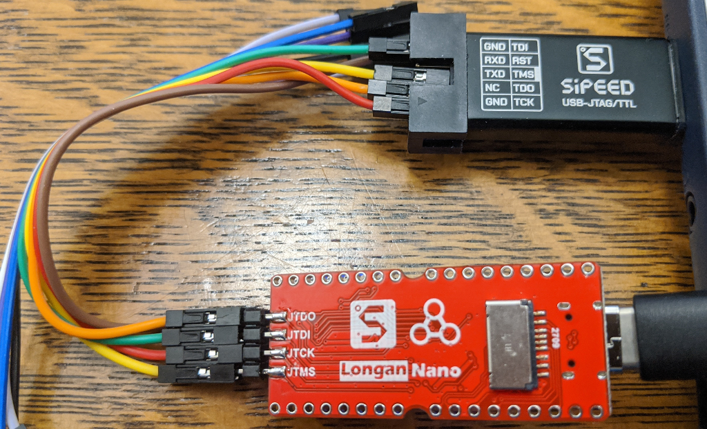
Longan Nano debugging connections – don’t forget the ‘Ground’ connection on the other side!
Once everything is wired together and plugged in, find the openocd_ft2232.cfg file in the GD32VF103 Firmware Library package’s Template/ directory, and run openocd with it. If it works, you should see something like this:
openocd -f openocd_ft2232.cfg
Open On-Chip Debugger [version]
Licensed under GNU GPL v2
For bug reports, read
	http://openocd.org/doc/doxygen/bugs.html
Info : clock speed 1000 kHz
Info : JTAG tap: riscv.cpu tap/device found: 0x1e200a6d (mfg: 0x536 (Nuclei System Technology Co.,Ltd.), part: 0xe200, ver: 0x1)
Info : JTAG tap: auto0.tap tap/device found: 0x790007a3 (mfg: 0x3d1 (GigaDevice Semiconductor (Beijing)), part: 0x9000, ver: 0x7)
Warn : AUTO auto0.tap - use "jtag newtap auto0 tap -irlen 5 -expected-id 0x790007a3"
Info : datacount=4 progbufsize=2
Info : Examined RISC-V core; found 1 harts
Info :  hart 0: XLEN=32, misa=0x40901105
Info : Listening on port 3333 for gdb connections
Info : Listening on port 6666 for tcl connections
Info : Listening on port 4444 for telnet connections
If you get an error like, Error: no device found, you might just need to remove the ftdi_device_desc "Dual RS232-HS" line from the configuration script and try again. And if you get an error like, Error: libusb_open() failed with LIBUSB_ERROR_ACCESS, you might need to either run openocd with sudo, or write a udev rule to provide more permissive access to the USB device.
Step 2: Boot Code
Now that you can build code for your chip and connect to it, it’s time to finally write some code. First, we’ll need the same basic building blocks that we learned about in the first couple of STM32 bare-metal examples that I wrote awhile ago:
- A linker script, to tell the linker how much RAM and Flash memory is available and where to put each of the program’s sections.
- A vector table, to define where in memory the program should boot from and where it should jump to for various interrupt handler functions.
- A ‘reset handler’ function, to perform basic initialization steps before ‘main’ is called.
And as usual, you can find working examples of these files in this post’s GitHub repository; most of these boot code files are in the common/ directory. Feel free to reach out if something seems broken – I always appreciate the feedback, and I’m sorry if I get distracted and it takes me awhile to respond.
Linker Script
First up is the linker script: this looks almost identical to the linker scripts which we’ve written for STM32 cores, because the GNU toolchain’s linker works pretty much the same across different platforms. I usually name linker scripts after the chip that they describe, like gd32vf103xb.ld:
OUTPUT_ARCH( "riscv" )
ENTRY( reset_handler )

MEMORY
{
  FLASH (rx)  : ORIGIN = 0x08000000, LENGTH = 128K
  RAM   (rwx) : ORIGIN = 0x20000000, LENGTH = 32K
}


SECTIONS
{
  __stack_size = DEFINED(__stack_size) ? __stack_size : 1K;

  .vector_table :
  {
    KEEP (*(SORT_NONE(.vector_table)))
  } >FLASH

  .text :
  {
    *(.rodata .rodata.*)
    *(.srodata .srodata.*)
    *(.text .text.*)
  } >FLASH

  . = ALIGN(4);

  PROVIDE (__etext = .);
  PROVIDE (_etext = .);
  PROVIDE (etext = .);

  _sidata = .;
  .data : AT( _sidata )
  {
    _sdata = .;
    *(.rdata)
    *(.data .data.*)
    *(.sdata .sdata.*)
    . = ALIGN(4);
    _edata = .;
  } >RAM

  PROVIDE( _edata = . );
  PROVIDE( edata = . );
  PROVIDE( _fbss = . );
  PROVIDE( __bss_start = . );

  .bss :
  {
    _sbss = .;
    *(.sbss*)
    *(.bss .bss.*)
    *(COMMON)
    . = ALIGN(4);
    _ebss = .;
  } >RAM

  . = ALIGN(8);
  PROVIDE( _end = . );
  PROVIDE( end = . );

  .stack ORIGIN(RAM) + LENGTH(RAM) - __stack_size :
  {
    PROVIDE( _heap_end = . );
    . = __stack_size;
    PROVIDE( _sp = . );
  } >RAM
}
No real surprises there – if it looks like gibberish, check my first couple of STM32 bare-metal examples for some more context on linker scripts. Also, you should know that most linker scripts for this chip seem to define a __global_pointer$ value in the .data section which I chose to omit. RISC-V supports a special ‘global pointer’ register which lets the toolchain perform optimizations known as ‘linker relaxation’, but I thought that might be confusing to include in these simple example programs, and it looks like the optimizations are only used if you explicitly set the gp register in your boot code. SiFive wrote a good article with more information on the subject, but it doesn’t seem useful for these introductory examples, and I think it is safe to ignore.
Vector Table
Next up is the vector table. Again, this looks very much like the assembly vector tables which you might use with other sorts of microcontrollers, but there are a few small differences from an STM32 vector table. First, there is no entry for an ‘end of stack’ value. We’ll still initialize the stack pointer to the end of usable RAM in our boot code, but we don’t need a separate vector table entry for it. And second, the first “reset handler” entry is actually a “Jump” assembly instruction instead of a memory address.
Finally, this is a very minor difference but I used the .set assembler directive instead of .thumb_set to create weak links for each vector table entry to the default interrupt handler. It does the same thing, but “Thumb” is the name of the instruction set used by ARM Cortex-M cores, so I don’t think that the RISC-V toolchain supports the .thumb_set syntax. I won’t copy every entry here to save space, but you can find the whole thing in the reference repository:
/*
 * Main vector table entries.
 */
.global vtable
.type vtable, %object
.section .vector_table,"a",%progbits
vtable:
  J reset_handler
  .align 2
  .word 0
  .word 0
  .word eclic_msip_handler
  .word 0
  .word 0
  .word 0
  .word eclic_mtip_handler
  .word 0
  .word 0
  .word 0
  .word 0
  .word 0
  .word 0
  .word 0
  .word 0
  .word 0
  .word eclic_bwei_handler
  .word eclic_pmovi_handler
  .word watchdog_IRQn_handler
  .word LVD_IRQn_handler
  .word tamper_IRQn_handler
  .word RTC_IRQn_handler
  .word FMC_IRQn_handler
  .word RCU_IRQn_handler
  .word EXTI0_IRQn_handler
  [...]
  .word USB_IRQn_handler

  /*
   * Weak aliases to point each exception hadnler to the
   * 'default_interrupt_handler', unless the application defines
   * a function with the same name to override the reference.
   */
  .weak eclic_msip_handler
  .set  eclic_msip_handler,default_interrupt_handler
  .weak eclic_mtip_handler
  .set  eclic_mtip_handler,default_interrupt_handler
  .weak eclic_bwei_handler
  .set  eclic_bwei_handler,default_interrupt_handler
  .weak eclic_pmovi_handler
  .set  eclic_pmovi_handler,default_interrupt_handler
  .weak watchdog_IRQn_handler
  .set  watchdog_IRQn_handler,default_interrupt_handler
  .weak LVD_IRQn_handler
  .set  LVD_IRQn_handler,default_interrupt_handler
  .weak tamper_IRQn_handler
  .set  tamper_IRQn_handler,default_interrupt_handler
  .weak RTC_IRQn_handler
  .set  RTC_IRQn_handler,default_interrupt_handler
  .weak FMC_IRQn_handler
  .set  FMC_IRQn_handler,default_interrupt_handler
  .weak RCU_IRQn_handler
  .set  RCU_IRQn_handler,default_interrupt_handler
  .weak EXTI0_IRQn_handler
  .set  EXTI0_IRQn_handler,default_interrupt_handler
  [...]
  .weak USB_IRQn_handler
  .set  USB_IRQn_handler,default_interrupt_handler

/*
 * A 'default' interrupt handler, in case an interrupt triggers
 * without a handler being defined.
 */
.section .text.default_interrupt_handler,"ax",%progbits
default_interrupt_handler:
    default_interrupt_loop:
      j default_interrupt_loop
I put this in a file called gd32vf103xb_boot.S, but you might want to pick something shorter.
Vendor-Provided System Header Files
ARM Cortex-M cores have a collection of CMSIS header files which define helper functions for the microcontroller’s CPU functions, like the SysTick and NVIC peripherals. This RISC-V CPU has a similar set of files, which you can find in the standard firmware library repository. These contain definitions for some RISC-V CPU registers which are still in the ‘proposal’ stage of being added to the standard, and helper functions to do things like configure the CPU’s interrupt handler.
I usually put these supporting files in a device_headers/ directory. The n200_ prefix refers to the specific kind of RISC-V CPU core which these microcontrollers use; the documentation calls it a “Bumblebee” core based on the “Nuclei N200” CPU implementation.
Reset Handler
The last bit of boot code that we need to write is a reset handler function, which sets up the chip’s memory space and calls the main method. When we wrote a simple STM32 reset handler, there wasn’t very much to do. First, we set the sp “stack pointer” register to the end of usable RAM space. Then, we copied the .data section of the program’s memory into RAM from the non-volatile Flash storage. Finally, we cleared the .bss section of the program’s memory to be all zeros. Once all of that is done, the chip’s memory space is in good shape to run the program, so we branched to the main C method to start the application.
We’ll do the same thing in our GD32V reset handler, with two small additions. First, we will clear a bit in one of the CPU’s CSRs (Control and Status Register) to disable hardware interrupts globally until the application configures them. Then, we’ll check if the program is running from a memory address of 0x0000... or 0x0800.... Our linker script thinks that the program is located in Flash memory which starts at 0x08000000 in the chip’s memory space, which is true, but some parts of these chips’ address space are “aliased” so that two memory addresses can refer to the same physical memory.
As I understand it, when the chip powers on and executes the first “Jump” instruction in the vector table, its pc “program counter” register will point to a memory address starting with 0x00000000, because that’s where the chip starts running from when it powers on. When the BOOT0 pin is held low, as it always is unless you are pressing the “Boot” button on the board, that address space is aliased to Flash memory, so executing code from 0x00001234 will run the code which you flashed to 0x08001234. But this often causes problems when your code try to access variables or constants, so we should jump from 0x0000... address space to 0x0800... very early in the program.
I could have some of that wrong, but it’s the best explanation I’ve been able to come up with after poking around in a debugger and seeing some odd memory corruption that only happened when the chip first powered on. Anyways, here’s an example reset handler function which you can put at the bottom of your gd32vf103xb_boot.S file:
/*
 * Assembly 'reset handler' function to initialize core CPU registers.
 */
.global reset_handler
.type reset_handler,@function
reset_handler:
  // Disable interrupts until they are needed.
  csrc CSR_MSTATUS, MSTATUS_MIE
  // Move from 0x00000000 to 0x08000000 address space if necessary.
  la   a0, in_address_space
  li   a1, 1
  slli a1, a1, 27
  bleu a1, a0, in_address_space
  add  a0, a0, a1
  jr   a0
  in_address_space:
  // Load the initial stack pointer value.
  la   sp, _sp
  // Set the vector table's base address.
  la   a0, vtable
  csrw CSR_MTVT, a0
  // Set non-vectored interrupts to use the default handler.
  // (That will gracefully crash the program,
  //  so only use vectored interrupts for now.)
  la   a0, default_interrupt_handler
  csrw CSR_MTVEC, a0
  // Call 'main(0,0)' (.data/.bss sections initialized there)
  li   a0, 0
  li   a1, 0
  call main
Besides switching address spaces and initializing the stack pointer, this reset handler sets a couple of CPU CSRs (Constrol and Status Registers). First, interrupts are disabled globally by clearing the MIE (Machine-mode Interrupts Enabled) bit in the MSTATUS CSR. The “Bumblebee” CPU core doesn’t necessarily reset all of its peripherals’ states with every kind of system reset, so it’s a good idea to clear any bits which your program might have previously enabled at the start of your application. And to prevent previously-enabled interrupts from erroneously triggering, it’s a good idea to clear the global interrupt enable flag before you do anything else.
The MTVT CSR contains the memory address of the vector table, which I annotated with the vtable label. You can also put your vector table in RAM to reduce interrupt latency a bit, but I didn’t do that here. And the upper 26 bits of the MTVEC CSR contains the aligned memory address of a “shared” reset handler which can be used to save and restore CPU or OS contexts – I’ll talk a little bit more about that later, but it’s a feature that I did not use in these example programs, so I pointed it at the default interrupt handler to prevent memory corruption if the shared interrupt handler is accidentally triggered.
I also decided not to set up the .data and .bss sections in the assembly code this time around, because I think it’s more legible to put calls to memcpy and memset at the top of the main method:
// Pre-defined memory locations for program initialization.
extern uint32_t _sidata, _sdata, _edata, _sbss, _ebss;
// 'main' method which gets called from the boot code.
int main( void ) {
  // Copy initialized data from .sidata (Flash) to .data (RAM)
  memcpy( &_sdata, &_sidata, ( ( void* )&_edata - ( void* )&_sdata ) );
  // Clear the .bss RAM section.
  memset( &_sbss, 0x00, ( ( void* )&_ebss - ( void* )&_sbss ) );

  // Endlessly increment a variable.
  volatile int counter = 0;
  while ( 1 ) {
    counter++;
  }
  return 0;
}
And that’s enough C code to test our debugging toolchain – once we’ve written a Makefile to build the program, we’ll be able to flash it with OpenOCD and verify that it runs properly with GDB.
Makefile
Again, a basic Makefile for these chips looks very similar to the ones that I’ve been using throughout the STM32 tutorials that I’ve written. Besides replacing the arm-none-eabi- prefix with riscv32-unknown-elf-, the flags which specify what sort of CPU architecture we’re using are also a bit different. And I passed the --no-relax option into the linker so that the gp “general pointer” register is not used, as I mentioned above. But otherwise, this example from the reference repository‘s hello_riscv example will probably look familiar if you’ve seen a few Makefiles:
# GCC toolchain programs.
CC = riscv32-unknown-elf-gcc
OC = riscv32-unknown-elf-objcopy
OS = riscv32-unknown-elf-size

# Assembly directives.
ASFLAGS += -c
ASFLAGS += -O0
ASFLAGS += -Wall
ASFLAGS += -fmessage-length=0
ASFLAGS += -march=rv32imac
ASFLAGS += -mabi=ilp32
ASFLAGS += -mcmodel=medlow

# C compilation directives
CFLAGS += -c
CFLAGS += -Wall
CFLAGS += -O0
CFLAGS += -g
CFLAGS += -fmessage-length=0
CFLAGS += --specs=nosys.specs
CFLAGS += -march=rv32imac
CFLAGS += -mabi=ilp32
CFLAGS += -mcmodel=medlow

# Linker directives.
LFLAGS += -Wall
LFLAGS += -Wl,--no-relax
LFLAGS += -Wl,--gc-sections
LFLAGS += -nostdlib
LFLAGS += -nostartfiles
LFLAGS += -lc
LFLAGS += -lgcc
LFLAGS += --specs=nosys.specs
LFLAGS += -march=rv32imac
LFLAGS += -mabi=ilp32
LFLAGS += -mcmodel=medlow
LFLAGS += -T./../common/gd32vf103xb.ld

# Source files.
AS_SRC  = ./../common/gd32vf103xb_boot.S
C_SRC   = ./main.c

# Header file directories.
INCLUDE = -I./../common/device_headers

# Object files to build.
OBJS  = $(AS_SRC:.S=.o)
OBJS += $(C_SRC:.c=.o)

# Default rule to build the whole project.
.PHONY: all
all: main.bin

# Rule to build assembly files.
%.o: %.S
  $(CC) -x assembler-with-cpp $(ASFLAGS) $(INCLUDE) $< -o $@

# Rule to compile C files.
%.o: %.c
  $(CC) $(CFLAGS) $(INCLUDE) $< -o $@

# Rule to create an ELF file from the compiled object files.
main.elf: $(OBJS)
  $(CC) $^ $(LFLAGS) -o $@

# Rule to create a raw binary file from an ELF file.
main.bin: main.elf
  $(OC) -S -O binary $< $@
  $(OS) $<

# Rule to clear out generated build files.
.PHONY: clean
clean:
  rm -f $(OBJS)
  rm -f main.elf
  rm -f main.bin
Once you run make, you should end up with the familiar main.bin and main.elf program files. If you’re having trouble following along or keeping track of file names (or if I made a typo somewhere), you can find a full example project in the reference repository‘s common/ and hello_riscv/ directories.
Debugging
Once your program is built, go ahead and open a debugging connection to the chip as described in the “OpenOCD” section under Step 1 above. Then, open your main.elf file with GDB:
>riscv32-unknown-elf-gdb -q main.elf
Reading symbols from main.elf...
(gdb)
The -q or “quiet” argument just asks GDB not to print most of its introductory text. If you have an active OpenOCD connection on the default port 3333, you should be able to tap into that connection with target extended-remote :3333 and flash your program to the chip with the load command. Then you can run your program and convince yourself that it works by following the same steps as you would with any other GDB debugging session. For example:
(gdb) target extended-remote :3333
Remote debugging using :3333
0x080001a2 in main () at src/main.c:35
35	  memcpy( &_sdata, &_sidata, ( ( void* )&_edata - ( void* )&_sdata ) );
(gdb) load
Loading section .vector_table, size 0x15c lma 0x8000000
Loading section .text, size 0x298 lma 0x800015c
Start address 0x800015e, load size 1012
Transfer rate: 975 bytes/sec, 506 bytes/write.
(gdb) backtrace
#0  reset_handler () at src/main.c:13
(gdb) break main
Breakpoint 1 at 0x8000194: file src/main.c, line 35.
(gdb) continue
Continuing.
Note: automatically using hardware breakpoints for read-only addresses.

Breakpoint 1, main () at src/main.c:35
35	  memcpy( &_sdata, &_sidata, ( ( void* )&_edata - ( void* )&_sdata ) );
(gdb) print counter
$1 = 536903680
(gdb) next
37	  memset( &_sbss, 0x00, ( ( void* )&_ebss - ( void* )&_sbss ) );
(gdb) next
40	  volatile int counter = 0;
(gdb) print counter
$2 = 0
(gdb) next
42	    counter++;
(gdb) continue
Continuing.
^C
Program received signal SIGINT, Interrupt.
0x080001f4 in main () at src/main.c:42
42	    counter++;
(gdb) print counter
$3 = 3389557
(gdb)
Here, you can see that after loading the program, the chip starts running the reset_handler function. If you set a breakpoint at the main method and print the counter variable, you can see why we need to clear the .bss section at the start of our program. When the chip first boots, its RAM could contain anything, so we need to initialize it before starting the main program. After the memset operation which clears the .bss section, the value is set to its expected starting value of zero. Then, after the program runs for a little while, you can see that it counts up over time.
So it looks like this boot code should work for a simple application. Let’s move on to lighting up the board’s RGB LED.
Step 3: Blinking LEDs
GPIO Configuration
Like I mentioned above, the GD32VF103 peripherals work almost the same as those on an STM32F103 chip. But the STM32F1 family of microcontrollers is a little bit older than the ones which I’ve been writing about, so some peripherals – including the GPIO pins – are configured differently.
The GPIO peripherals don’t use four separate registers to configure the pin’s mode, pull-up/down resistors, output speed, and output type. Instead, they use four bits to define each pin’s configuration, split between two ‘mode’ bits and two ‘configuration’ bits. Those bits are split across two 32-bit registers; CRL controls the ‘Low’ pins (0 through 7) and CRH controls the ‘High’ pins (8 through 15). The reference manual has a nice table showing how to set the bits for different pin configurations in section 7.3, but to drive an LED, we can set the ‘mode’ bits to 2 for a low-speed output and the ‘configuration’ bits to 0 to make it a general-purpose push-pull output.
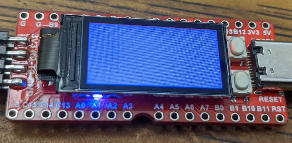
And as usual, you’ll need to use the chip’s “clock control” peripheral to enable the appropriate GPIOx peripherals before you configure any pins. You can check the Longan Nano’s schematics to see how the LEDs are wired; these boards include a common-anode RGB LED with the cathodes wired to pins A1 (Green), A2 (Blue), and C13 (Red).
Since the pins are wired to the cathodes of the LEDs instead of the anodes, each LED will turn off when the pin is pulled high and on when the pin is pulled low. It’s easy to get confused when LEDs are wired backwards like this, but it helps to remember that LEDs will light up when the voltage at their anode is higher than the voltage at their cathode. And I have an easy way to remember the difference between an LED’s cathode (-) and its anode (+): cats are lazy, so cathodes are usually closer to ground 🙂
Anyways, once you configure the GPIO pins as outputs, you can toggle them by writing to the peripheral’s ODR (Output Data Register) just like with an STM32. Here’s an example main method which cycles the LED through a few colors by individually toggling the red / green / blue colors:
#include "gd32vf103xb.h"

// Simple 'busy loop' delay method.
__attribute__( ( optimize( "O0" ) ) )
void delay_cycles( uint32_t cyc ) {
  uint32_t d_i;
  for ( d_i = 0; d_i < cyc; ++d_i ) {
    __asm__( "nop" );
  }
}

// Pre-defined memory locations for program initialization.
extern uint32_t _sidata, _sdata, _edata, _sbss, _ebss;
// 'main' method which gets called from the boot code.
int main( void ) {
  // Copy initialized data from .sidata (Flash) to .data (RAM)
  memcpy( &_sdata, &_sidata, ( ( void* )&_edata - ( void* )&_sdata ) );
  // Clear the .bss RAM section.
  memset( &_sbss, 0x00, ( ( void* )&_ebss - ( void* )&_sbss ) );

  // Enable the GPIOA and GPIOC peripherals.
  RCC->APB2ENR |=  ( RCC_APB2ENR_IOPAEN |
                     RCC_APB2ENR_IOPCEN );

  // Configure pins A1, A2, and C13 as low-speed push-pull outputs.
  GPIOA->CRL   &= ~( GPIO_CRL_MODE1 | GPIO_CRL_CNF1 |
                     GPIO_CRL_MODE2 | GPIO_CRL_CNF2 );
  GPIOA->CRL   |=  ( ( 0x2 << GPIO_CRL_MODE1_Pos ) |
                     ( 0x2 << GPIO_CRL_MODE2_Pos ) );
  GPIOC->CRH   &= ~( GPIO_CRH_MODE13 | GPIO_CRH_CNF13 );
  GPIOC->CRH   |=  ( 0x2 << GPIO_CRH_MODE13_Pos );

  // Turn all three LEDs off.
  // The pins are connected to the LED cathodes, so pulling
  // the pin high turns the LED off, and low turns it on.
  GPIOA->ODR   |=  ( 0x1 << 1 |
                     0x1 << 2 );
  GPIOC->ODR   |=  ( 0x1 << 13 );

  // Cycle the RGB LED through a pattern of colors.
  #define DELAY_CYCLES ( 300000 )
  while( 1 ) {
    // Green on (Green)
    GPIOA->ODR &= ~( 0x1 << 1 );
    delay_cycles( DELAY_CYCLES );
    // Red on (Yellow)
    GPIOC->ODR &= ~( 0x1 << 13 );
    delay_cycles( DELAY_CYCLES );
    // Blue on (White)
    GPIOA->ODR &= ~( 0x1 << 2 );
    delay_cycles( DELAY_CYCLES );
    // Green off (Purple)
    GPIOA->ODR |=  ( 0x1 << 1 );
    delay_cycles( DELAY_CYCLES );
    // Red off (Blue)
    GPIOC->ODR |=  ( 0x1 << 13 );
    delay_cycles( DELAY_CYCLES );
    // Blue off (Off)
    GPIOA->ODR |=  ( 0x1 << 2 );
    delay_cycles( DELAY_CYCLES );
  }
  return 0;
}
If you’ve read my previous STM32 posts or written bare-metal STM32 code before, this probably looks familiar. But the reason it looks familiar is because I also wrote a quick gd32vf103xb.h device header file which uses the same naming conventions that the STM32 ones do. The peripheral addresses and offsets are almost identical, but the two vendors often use different names for the same bits. So if you want to write platform-independent code which targets both STM32F1 and GD32VF1 chips, it looks like you’ll need to spend a little bit of time juxtaposing the two reference manuals.
So if you follow along in the reference manual, you’ll notice some naming discrepencies between my code and the GD32VF103 documentation. For example, they name the RCC peripheral RCU, and they start numbering peripherals from 0 instead of 1. For the sake of not using two naming schemes for one peripheral API, I’m going to stick with STM32 names when the API seems to work the same way. You can find the full (but still very incomplete) header file in the reference repository, but here’s an excerpt to give you the basic idea:
/**
 * RCC / RCU peripheral struct.
 */
typedef struct
{
  volatile uint32_t CR;
  volatile uint32_t CFGR;
  volatile uint32_t CIR;
  volatile uint32_t APB2RSTR;
  volatile uint32_t APB1RSTR;
  volatile uint32_t AHBENR;
  volatile uint32_t APB2ENR;
  volatile uint32_t APB1ENR;
  volatile uint32_t BDCR;
  /* The following registers differ from STM32F1: */
  volatile uint32_t RSTSCK;
  volatile uint32_t AHBRSTR;
  volatile uint32_t CFGR1;
  volatile uint32_t DSV;
} RCC_TypeDef;

/**
 * GPIO peripheral struct.
 */
typedef struct
{
  volatile uint32_t CRL;
  volatile uint32_t CRH;
  volatile uint32_t IDR;
  volatile uint32_t ODR;
  volatile uint32_t BSRR;
  volatile uint32_t BRR;
  volatile uint32_t LCKR;
} GPIO_TypeDef;

/* Global register block address definitions. */
#define RCC   ( ( RCC_TypeDef * )  0x40021000 )
#define GPIOA ( ( GPIO_TypeDef * ) 0x40010800 )
#define GPIOB ( ( GPIO_TypeDef * ) 0x40010C00 )
#define GPIOC ( ( GPIO_TypeDef * ) 0x40011000 )
#define GPIOD ( ( GPIO_TypeDef * ) 0x40011400 )
#define GPIOE ( ( GPIO_TypeDef * ) 0x40011800 )

/* RCC register bit definitions. */
/* APB2ENR */
#define RCC_APB2ENR_AFIOEN_Pos ( 0U )
#define RCC_APB2ENR_AFIOEN_Msk ( 0x1UL << RCC_APB2ENR_AFIOEN_Pos )
#define RCC_APB2ENR_AFIOEN     ( RCC_APB2ENR_AFIOEN_Msk )
#define RCC_APB2ENR_IOPAEN_Pos ( 2U )
#define RCC_APB2ENR_IOPAEN_Msk ( 0x1UL << RCC_APB2ENR_IOPAEN_Pos )
#define RCC_APB2ENR_IOPAEN     ( RCC_APB2ENR_IOPAEN_Msk )
#define RCC_APB2ENR_IOPBEN_Pos ( 3U )
#define RCC_APB2ENR_IOPBEN_Msk ( 0x1UL << RCC_APB2ENR_IOPBEN_Pos )
#define RCC_APB2ENR_IOPBEN     ( RCC_APB2ENR_IOPBEN_Msk )
//[...]

/* GPIO register bit definitions. */
/* CRL */
#define GPIO_CRL_MODE_Pos   ( 0U )
#define GPIO_CRL_MODE_Msk   ( 0x33333333UL << GPIO_CRL_MODE_Pos )
#define GPIO_CRL_MODE       ( GPIO_CRL_MODE_Msk )
#define GPIO_CRL_MODE0_Pos  ( 0U )
#define GPIO_CRL_MODE0_Msk  ( 0x3UL << GPIO_CRL_MODE0_Pos )
#define GPIO_CRL_MODE0      ( GPIO_CRL_MODE0_Msk )
#define GPIO_CRL_MODE1_Pos  ( 4U )
#define GPIO_CRL_MODE1_Msk  ( 0x3UL << GPIO_CRL_MODE1_Pos )
#define GPIO_CRL_MODE1      ( GPIO_CRL_MODE1_Msk )
//[...]
#define GPIO_CRL_CNF_Pos    ( 2U )
#define GPIO_CRL_CNF_Msk    ( 0x33333333UL << GPIO_CRL_CNF_Pos )
#define GPIO_CRL_CNF        ( GPIO_CRL_CNF_Msk )
#define GPIO_CRL_CNF0_Pos   ( 2U )
#define GPIO_CRL_CNF0_Msk   ( 0x3UL << GPIO_CRL_CNF0_Pos )
#define GPIO_CRL_CNF0       ( GPIO_CRL_CNF0_Msk )
#define GPIO_CRL_CNF1_Pos   ( 6U )
#define GPIO_CRL_CNF1_Msk   ( 0x3UL << GPIO_CRL_CNF1_Pos )
#define GPIO_CRL_CNF1       ( GPIO_CRL_CNF1_Msk )
//[...]
I’m not sure if it’s worth keeping the same _Pos (“Position”) and _Msk (“Mask”) syntax for the bitfields, and I omitted some even more granular bit definitions like GPIO_CRL_CNF_MODE0_0. It’s usually not good to be choosy when you’re trying to maintain compatibility with older code, but I doubt anyone actually uses most of these macros and it’d be nice to have some more human-readable names for multi-bit fields. I guess that’s what a HAL is for though, and anyways, a better long-term solution would be to auto-generate this sort of file from the .svd (System View Description) files which are provided by the chip vendor.
So you can check the hello_led project in the reference repository to see a full project which implements the above code, or you can update your project if you’ve been following along. When you flash the resulting program, the board’s LED should start cycling through a few different colors.
The Longan Nano’s RGB LED is located underneath the board’s display, but you should be able to see it pretty easily once it lights up 🙂
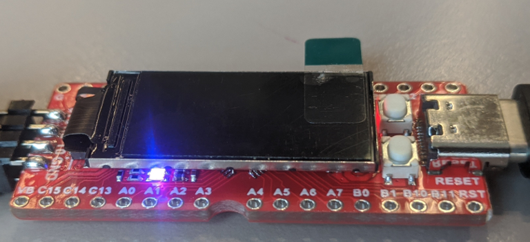
This is where I learned about the need to jump from 0x0000... to 0x0800... address space in the reset handler. When I power-cycled the board for the first time after flashing this program, the LEDs would all light up without changing color. When I looked in a debugger, the code was running properly but the stack pointer addresses were all wrong, usually around 0x18... instead of 0x20....
Some of the registers and saved stack values also seemed to refer to read-only memory addresses without their 0x0800 prefixes, so I figure that the power-on-reset logic must not automatically relocate the program into the right virtual memory space. It looked like the LEDs weren’t changing colors because 0xFFFFFFFF was getting passed into the delay_cycles method, which also smelled like memory corruption.
Anyways, adding the small bit of assembly code which jumps forward by 0x08000000 if necessary seems to have fixed the issue, but I’d be interested in hearing ideas if you think it was caused by something else. Now, before we move on to drawing to the board’s TFT display, let’s see how interrupts work by using the CPU’s internal timer to generate some more precisely-timed delays.
System Timer Interrupt Configuration
This particular kind of RISC-V CPU controls its hardware interrupts using a peripheral which it calls ECLIC (Enhanced Core-Level Interrupt Controller), so we’ll need to enable and configure that if we want to set up the CPU timer interrupt to increment a counter every millisecond.
The ECLIC peripheral can actually be configured in one of two different modes for each individual interrupt. The “vectored” interrupt mode works very similarly to ARM Cortex-M interrupts: it simply checks the vector table to see where the appropriate interrupt handler is located in memory, then it jumps to that interrupt handler.
But unlike ARM Cortex-M CPUs, this type of RISC-V CPU doesn’t have specialized hardware for saving and restoring the CPU’s context before and after an interrupt handler runs. We can ask the compiler to auto-generate the small amount of code which does that by annotating interrupt handler functions with __attribute__( ( interrupt ) ), but there’s still a bit of extra helper code that you’ll need to provide if you want higher-priority interrupts to be able to interrupt lower-priority ones. You can read more about that in the “Vector processing mode” section of the CPU core’s datasheet (section 5.13.2 at the time of writing), but suffice to say, the “vectored” interrupt handling mode comes with a few caveats in these “Bumblebee” RISC-V CPU cores.
To help with that, there is an alternate “non-vectored” interrupt mode. All interrupts which are configured as “non-vectored” will jump to the same common interrupt handler, which can perform context saving and restoring actions before and after calling the appropriate interrupt handler function. The standard firmware library uses this “non-vectored” mode, but this post is already getting pretty long, so I’m going to use the simpler “vectored” interrupt mode to cut down on explanations and assembly code sections. That’s why I set the upper 26 bits of the MTVEC CSR to the “default interrupt handler” address in the reset handler; those bits normally hold the location of the shared exception handler, which I did not implement.
I don’t think that the process for configuring vectored interrupts is very different from configuring non-vectored ones, though. You just need to add a call to eclic_set_vmode( interrupt_number );. So combined with the initialization steps which are already performed in the reset handler, this block of code should enable the ECLIC peripheral and set up the system timer interrupt:
// Set up the global timer to generate an interrupt every ms.
// Figure out how many interrupts are available.
uint32_t max_irqn = *( volatile uint32_t * )( ECLIC_ADDR_BASE + ECLIC_INFO_OFFSET );
max_irqn &= ( 0x00001FFF );
// Initialize the 'ECLIC' interrupt controller.
eclic_init( max_irqn );
eclic_mode_enable();
// Set 'vector mode' so the timer interrupt uses the vector table.
eclic_set_vmode( CLIC_INT_TMR );
// Enable the timer interrupt with low priority and 'level'.
eclic_enable_interrupt( CLIC_INT_TMR );
eclic_set_irq_lvl_abs( CLIC_INT_TMR, 1 );
eclic_set_irq_priority( CLIC_INT_TMR, 1 );
Some functions, like eclic_init, are located in the n200_func.c file, so you’ll also need to add that to the C_SRC variable in your Makefile. Unlike with ARM Cortex-M cores, the “Nuclei N200” system functions don’t all fit into a few header files; there’s also one extra C file that we need to include.
Note that the eclic_init function needs to be told how many interrupt handler entries the CPU has; while we could hard-code that value, according to the “Bumblebee” processor’s reference manual‘s “Eclic register” section (6.2.5 at the time of writing), we can also find the expected size of the chip’s vector table by checking bits [0:12] in the clicinfo register.
Once we have initialized the ECLIC peripheral, we can configure the CPU’s timer to generate interrupts after a specified number of cycles by writing to the mtimecmp_lo and mtimecmp_hi registers. The system timer is a 64-bit counter, so all of its counter settings span two 32-bit “high” and “low” registers. But those registers are right next to each other, so you can address them as a pointer to a volatile uint64_t in your C code. And it’s also a good idea to reset the MTIME value to zero before setting the MSTATUS_MIE bit to enable interrupts globally, so that the interrupt doesn’t immediately trigger.
Putting all of that together, you can configure the system timer interrupt to trigger every millisecond and start the timer like this:
// Set the timer's comparison value to (frequency / 1000).
*( volatile uint64_t * )( TIMER_CTRL_ADDR + TIMER_MTIMECMP ) = ( TIMER_FREQ / 1000 );
// Reset the timer value to zero.
*( volatile uint64_t * )( TIMER_CTRL_ADDR + TIMER_MTIME ) = 0;
// Re-enable interrupts globally.
set_csr( mstatus, MSTATUS_MIE );
The TIMER_FREQ macro is set in the n200_timer.h header file, and it is set to SystemCoreClock / 4. These system files seem to follow the standard of expecting a global “core clock frequency” variable which is named SystemCoreClock, so you’ll need to make sure that is defined in your application. In the reference repository‘s hello_systick example, the value is declared in the gd32vf103.h device header file and initialized to its default value of 8MHz near the top of the main.c file.
Finally, we can define a global volatile uint32_t systick variable near the top of our main.c file and set up an interrupt handler function to increment it:
// Global 'tick' value.
volatile uint32_t systick = 0;

// [...]

// System timer interrupt.
__attribute__( ( interrupt ) )
void eclic_mtip_handler( void ) {
  // Increment the global 'tick' value.
  systick++;
  // Reset the 'mtime' value to zero.
  *( volatile uint64_t * )( TIMER_CTRL_ADDR + TIMER_MTIME ) = 0;
}
Then we can use the global systick value to write a more precise “delay” function which waits a specified number of milliseconds:
// Simple "millisecond delay" function.
void delay_ms( uint32_t ms ) {
  // Calculate the 'system tick' value to wait until.
  uint32_t done = systick + ms;
  // Wait until the 'systick' value ticks up enough.
  while ( systick < done ) { __WFI(); }
}
Most CPU cores let you save a bit of power without much effort by calling some sort of WFI “Wait For Interrupt” macro when you expect the chip to remain idle until some hardware interrupt triggers, and these RISC-V chips are no exception. So we can use a bit less energy while idling by calling __WFI(); instead of __asm__( "nop" ); in this sort of situation.
If you add all of that to your project and replace the calls to delay_cycles with delay_ms, your LEDs should cycle through colors with predictably-timed delays based on the system timer’s interrupt instead of an imprecise ‘busy loop’. Remember that you can find example code in the hello_systick project in the reference repository…although, the peripheral is called TIMER instead of SysTick in the CPU’s reference manual. Nevermind, let’s move on and draw to the board’s TFT display!
Step 4: Display DMA
The Longan Nano board uses a 160×80-pixel ST7735 display with 16 bits of color per pixel and a fairly standard SPI interface. It uses SPI clock, SPI data, “chip select”, “reset”, and “data / command” signals, so you’ll need to configure a total of five GPIO pins. The SPI data signal is bi-directional, but this example code will treat the display as write-only to make things less complicated.
If you read my earlier post about the DMA peripheral on various STM32 chips, this display seems to accept commands which are almost identical to those used by the ILI9341 and ILI9163C displays which I used as examples there. You can find a complete example application in the reference repository‘s hello_display example, and you can find more information about the initialization commands in section 10 of the display controller’s datasheet.
But another difference between the newer STM32 peripherals which I’ve talked about previously and the time-tested STM32F1 / GD32VF1 ones is how the ‘alternate function’ GPIO settings are configured. Most of these chips’ GPIO pins only map to one or two peripherals, so there are no ‘alternate function’ bits in the GPIO peripheral to select which peripheral each pin should connect to. Instead, you just set the pin mode to ‘alternate function’ instead of ‘general purpose’. There are a handful of “remap” bits in the AFIO (Alternate Function Input/Output) registers, but you only need to use them if you want to configure a secondary pin/peripheral mapping.
The Longan Nano uses pin A5 for the SPI clock signal, A7 for SPI data, B0 for “data / command”, B1 for “reset”, and B2 for “chip select”. That corresponds to the SPI0 peripheral, which I call SPI1 to maintain compatibility with STM32F1 code. The SPI0_REMAP bit switches the associated GPIO pins from A4/A5/A6/A7 to A15/B3/B4/B5, so we should leave it un-set. If you configure the “chip select”, “data / command”, and “reset” pins as low-speed push-pull outputs, your RCC and GPIO configuration code can look something like this:
// Enable the GPIOA, GPIOB, GPIOC, SPI1, and DMA1 peripherals.
RCC->APB2ENR  |=  ( RCC_APB2ENR_IOPAEN |
                    RCC_APB2ENR_IOPBEN |
                    RCC_APB2ENR_IOPCEN |
                    RCC_APB2ENR_SPI1EN );
RCC->AHBENR   |=  ( RCC_AHBENR_DMA1EN );

// Configure pins A1, A2, and C13 as low-speed push-pull outputs.
GPIOA->CRL    &= ~( GPIO_CRL_MODE1 | GPIO_CRL_CNF1 |
                    GPIO_CRL_MODE2 | GPIO_CRL_CNF2 );
GPIOA->CRL    |=  ( ( 0x2 << GPIO_CRL_MODE1_Pos ) |
                    ( 0x2 << GPIO_CRL_MODE2_Pos ) );
GPIOC->CRH    &= ~( GPIO_CRH_MODE13 | GPIO_CRH_CNF13 );
GPIOC->CRH    |=  ( 0x2 << GPIO_CRH_MODE13_Pos );
// Configure pins A5 and A7 as high-speed alternate-function outputs.
GPIOA->CRL    &= ~( GPIO_CRL_MODE5 | GPIO_CRL_CNF5 |
                    GPIO_CRL_MODE7 | GPIO_CRL_CNF7 );
GPIOA->CRL    |=  ( ( 0x3 << GPIO_CRL_MODE5_Pos ) |
                    ( 0x3 << GPIO_CRL_MODE7_Pos ) |
                    ( 0x2 << GPIO_CRL_CNF5_Pos ) |
                    ( 0x2 << GPIO_CRL_CNF7_Pos ) );
// Configure pins B0, B1, and B2 as low-speed push-pull outputs.
GPIOB->CRL    &= ~( ( GPIO_CRL_MODE0 | GPIO_CRL_CNF0 ) |
                    ( GPIO_CRL_MODE1 | GPIO_CRL_CNF1 ) |
                    ( GPIO_CRL_MODE2 | GPIO_CRL_CNF2 ) );
GPIOB->CRL    |=  ( ( 0x2 << GPIO_CRL_MODE0_Pos ) |
                    ( 0x2 << GPIO_CRL_MODE1_Pos ) |
                    ( 0x2 << GPIO_CRL_MODE2_Pos ) );
You might be tempted to use high-speed push-pull outputs for the “reset”, “data / command”, and “chip select” pins, but lower speeds often generate less electromagnetic ‘noise’, and there wouldn’t be much point to using higher speeds for this application. The “reset” pin will only be toggled once at the beginning of the program to restart the display, the “data / command” pin will remain in the “data” position after we configure the display and set up a circular DMA transfer, and the “chip select” pin will also stay in the “active” position most of the time.
You can configure the DMA peripheral as what I called a “Type 1” DMA channel in my STM32 DMA post; happily, the DMA and SPI peripherals don’t seem to have changed much in the 10+ years since the STM32F1 series was released. I guess it makes sense; the underlying ideas and standards are even older.
// Framebuffer for the TFT display.
// (Outside of your 'main' method)
#define TFT_W ( 160 )
#define TFT_H ( 80 )
#define TFT_A ( TFT_W * TFT_H )
volatile uint16_t fb[ TFT_A ];

// DMA configuration (Inside of your 'main' method):
// - Memory-to-peripheral mode.
// - Circular mode enabled for continuous transfer.
// - Increment source ptr, don't increment destination ptr.
// - 8-bit transfer length.
// - High-priority. Not that priority matters; it's the only one.
DMA1_Channel3->CCR  &= ~( DMA_CCR_MEM2MEM |
                          DMA_CCR_PL |
                          DMA_CCR_MSIZE |
                          DMA_CCR_PSIZE |
                          DMA_CCR_PINC |
                          DMA_CCR_EN );
DMA1_Channel3->CCR  |=  ( ( 0x2 << DMA_CCR_PL_Pos ) |
                          DMA_CCR_MINC |
                          DMA_CCR_CIRC |
                          DMA_CCR_DIR );
// Set source memory address to the framebuffer array.
DMA1_Channel3->CMAR  =  ( uint32_t )&( fb );
// Set destination peripheral address to the SPI1 data register.
DMA1_Channel3->CPAR  =  ( uint32_t )&( SPI1->DR );
// Set the number of bits to transfer. In this case, it's the
// number of 16-bit colors multiplied by two.
DMA1_Channel3->CNDTR =  ( uint32_t )( TFT_A * 2 );
The SPI1 peripheral’s “transmit” DMA connection is mapped to DMA1_Channel3, just like with STM32F1 chips. But remember that the GD32VF documentation starts numbering its peripherals at zero, so it refers to these signals as SPI0_TX and DMA0_Channel2. Sorry again for the confusion.
Next is the SPI configuration, which might also look familiar if you’ve ready any of my previous posts which used the SPI peripheral:
// SPI1 setup: host mode, no baud rate division, sw cs pin control,
// TX DMA enabled, 8-bit frames, msb-first, enable the peripheral.
// Some of those settings are the default state after a reset.
SPI1->CR2  |=  ( SPI_CR2_TXDMAEN );
SPI1->CR1  &= ~( SPI_CR1_BR );
SPI1->CR1  |=  ( SPI_CR1_SSM |
                 SPI_CR1_SSI |
                 SPI_CR1_MSTR |
                 SPI_CR1_SPE );
The TXDMAEN bit causes the SPI peripheral to request a new ‘transmit’ DMA transfer every time that its output buffer is empty. We still need to send a few initialization commands before starting the DMA transfer, but that’s okay because the DMA peripheral won’t respond to the SPI peripheral’s requests until we set the appropriate DMA_CCR_EN bit.
After everything is configured, it’s also a good idea to set up the initial states for the display interface’s software-controlled pins (reset, data / command, and chip select):
// Set initial SPI pin positions.
// Pull the 'chip select' pin high to de-select the display.
GPIOB->ODR |=  ( 0x1 << 2 );
// Pull the 'reset' pin low to reset the display.
GPIOB->ODR &= ~( 0x1 << 1 );
// Wait 100ms and pull the 'reset' pin high.
delay_ms( 100 );
GPIOB->ODR |=  ( 0x1 << 1 );
// Pull the 'chip select' pin low to get the display's attention.
GPIOB->ODR &= ~( 0x1 << 2 );
The ‘data’ and ‘clock’ pins will be automatically controlled by the peripheral. Now that the SPI peripheral is set up, you can write a few helper functions to send data and commands to the chip. These also look similar to the helper methods in the post that I wrote about SPI TFT displays. First, you’ll want one to switch modes with the “data / command” pin:
// 'Switch data/command mode' display helper function.
#define MODE_CMD ( 0 )
#define MODE_DAT ( 1 )
void display_mode( int type ) {
  // Wait for any ongoing transfers to finish.
  while ( SPI1->SR & SPI_SR_BSY ) {};
  // Set the 'data / command' pin level.
  if ( type ) { GPIOB->ODR |=  ( 0x1 << 0 ); }
  else        { GPIOB->ODR &= ~( 0x1 << 0 ); }
}
Then, you’ll want functions to write 8-bit and 16-bit values to the display:
// 'Write SPI byte' display helper function.
void spi_w8( SPI_TypeDef* SPIx, uint8_t byte ) {
  // Wait for the transmit buffer to have space.
  while ( !( SPI1->SR & SPI_SR_TXE ) ) {};
  // Send the next byte of data.
  *( uint8_t * )&( SPIx->DR ) = byte;
}

// 'Write SPI half-word' display helper function.
void spi_w16( SPI_TypeDef* SPIx, uint16_t hword ) {
  spi_w8( SPIx, hword >> 8 );
  spi_w8( SPIx, hword & 0xFF );
}
With those helper functions set up, you can send a basic minimal initialization sequence after your peripherals are configured in your main method:
// Send initialization commands to the display before starting DMA.
// Software reset.
display_mode( MODE_CMD );
spi_w8( SPI1, 0x01 );
delay_ms( 100 );
// Display off.
spi_w8( SPI1, 0x28 );
// 'Inverted' color mode, so that 0 is 'off' and 1 is 'on':
spi_w8( SPI1, 0x21 );
// Color mode: 16bpp.
spi_w8( SPI1, 0x3A );
display_mode( MODE_DAT );
spi_w8( SPI1, 0x05 );
// Memory access control.
display_mode( MODE_CMD );
spi_w8( SPI1, 0x36 );
display_mode( MODE_DAT );
spi_w8( SPI1, 0x20 );
// Exit sleep mode.
display_mode( MODE_CMD );
spi_w8( SPI1, 0x11 );
delay_ms( 100 );
// Display on.
spi_w8( SPI1, 0x29 );
delay_ms( 100 );
// Set drawing window.
// Column set
spi_w8( SPI1, 0x2A );
display_mode( MODE_DAT );
spi_w16( SPI1, 1 );
spi_w16( SPI1, TFT_W );
// Row set
display_mode( MODE_CMD );
spi_w8( SPI1, 0x2B );
display_mode( MODE_DAT );
spi_w16( SPI1, 26 );
spi_w16( SPI1, TFT_H + 25 );
// Set 'write to RAM' mode.
display_mode( MODE_CMD );
spi_w8( SPI1, 0x2C );
// Set 'data' transfer mode to start sending pixel data.
display_mode( MODE_DAT );
After the 0x29 “Display on” command, the display should light up with a rainbow of garbage data:
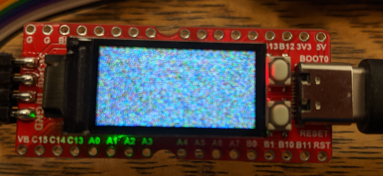
That static-y color is just the random values which were sitting in the display controller’s RAM when it started up.
If it doesn’t, check your GPIO / SPI / etc. initialization code against the reference repository. Once the display powers on properly, you can enable DMA to start sending the framebuffer, which should clear the display to black since the framebuffer array is probably located in the .bss section which gets set to zero at the start of the program. I also set the LSBFIRST bit in the SPI peripheral at this point, because it makes it easier to format the 16-bit RGB colors in memory:
// Set 'LSBFIRST' mode to make it easier to set color values.
SPI1->CR1          |=  ( SPI_CR1_LSBFIRST );
// Enable the circular DMA transfer.
DMA1_Channel3->CCR |=  ( DMA_CCR_EN );
Circular DMA transfers continue to run until you tell them to stop, so from now on, any colors that you write to the framebuffer array will quickly be reflected on the display. We didn’t re-configure the system clock, so it’s only running at 8MHz out of the chip’s top speed of 108MHz, but the refresh rate still seems pretty fast. Here’s a quick sample “main loop” which cycles the display and LED through a few different colors:
// Cycle the display through a few solid colors.
#define PATTERN_DELAY ( 1000 )
while( 1 ) {
  // Red (5 most-significant bits)
  for ( uint32_t i = 0; i < TFT_A; ++i ) {
    fb[ i ] = 0xF800;
  }
  GPIOA->ODR |=  ( 0x1 << 1 |
                   0x1 << 2 );
  GPIOC->ODR &= ~( 0x1 << 13 );
  delay_ms( PATTERN_DELAY );
  // Yellow
  for ( uint32_t i = 0; i < TFT_A; ++i ) {
    fb[ i ] = 0xFFE0;
  }
  GPIOA->ODR &= ~( 0x1 << 1 );
  GPIOA->ODR |=  ( 0x1 << 2 );
  GPIOC->ODR &= ~( 0x1 << 13 );
  delay_ms( PATTERN_DELAY );
  // Green (6 middle bits)
  for ( uint32_t i = 0; i < TFT_A; ++i ) {
    fb[ i ] = 0x03E0;
  }
  GPIOA->ODR &= ~( 0x1 << 1 );
  GPIOA->ODR |=  ( 0x1 << 2 );
  GPIOC->ODR |=  ( 0x1 << 13 );
  delay_ms( PATTERN_DELAY );
  // Purple
  for ( uint32_t i = 0; i < TFT_A; ++i ) {
    fb[ i ] = 0xF81F;
  }
  GPIOA->ODR |=  ( 0x1 << 1 );
  GPIOA->ODR &= ~( 0x1 << 2 );
  GPIOC->ODR &= ~( 0x1 << 13 );
  delay_ms( PATTERN_DELAY );
  // Blue (5 least-significant bits)
  for ( uint32_t i = 0; i < TFT_A; ++i ) {
    fb[ i ] = 0x001F;
  }
  GPIOA->ODR |=  ( 0x1 << 1 );
  GPIOA->ODR &= ~( 0x1 << 2 );
  GPIOC->ODR |=  ( 0x1 << 13 );
  delay_ms( PATTERN_DELAY );
}
It would be better to write functions like “fill rectangle” and “draw line” for the framebuffer, but there are plenty of existing libraries for that, and this is just a proof of concept to learn about how the microcontroller works. Anyways, if you run the above code (or the hello_display project in the reference repository), the display and LED should both cycle through a few solid colors:
That is one colorful board 🙂
Conclusions
This was fun! It’s cool to see a modern spin on the STM32F1 family of chips which is faster, probably more power-efficient, and largely API-compatible. And these GD32VF1 chips do seem like a good RISC-V learning platform, especially since Seeed Studios also sells cheap compatible JTAG debuggers which makes it easier to get started from scratch. But it is a little bit annoying that you need to write code to handle some of the intricacies of interrupt handling and memory space organization which ARM Cortex-M cores take care of automatically.
Also, sorry that I haven’t had time to write much over the past few months. I’ve been road-tripping around the United States, which is a lot of fun but also pretty distracting. The solar panels which I put on my car worked really well to keep all of my stuff charged, but I always have trouble convincing myself to be productive when I’m in a national park or forest. Maybe I’ll post some pictures soon if I can find a good way to format that, but I am also hoping to get back to electronics projects over the next few months. So hopefully I’ll have some time to make progress on the GPS handheld that I’ve been working on and finally write a basic UART tutorial soon. But I have also really grown to like the outdoors, which means that progress might be slow.

Ross Whenmouth
August 28, 2020 at 5:58 pm
I had trouble building riscv-openocd from https://github.com/riscv-mcu/riscv-openocd
So I have backported the GD32VF103 flash driver into mainline riscv-openocd.
It seems to work ok with my Longan Nano (I can read, erase and write to flash).
I have submitted a pull request https://github.com/riscv/riscv-openocd/pull/518 but in the interim, you can clone my code from here: https://github.com/ZL2WRW/riscv-openocd
Vivonomicon
September 6, 2020 at 12:59 pm
Oh, nice – that’s great to hear. It was sort of annoying to have to use a forked version of such a common utility. I should update the post to include that (although sometimes it takes me awhile to get around to updating old posts).
Thanks for the information and for porting that!
Matias
September 8, 2020 at 10:24 am
Hi, did you have issues with reset from the debugger? If I add “reset” keyword to openocd “program” command, the reset times out. I understand that it is not possible to reset the chip using JTAG protocol due to some limitation but the debugger has a RST pin and the Longan also, so I think it should be possible to configure openocd to make the debugger reset the chip from this pin, but I’m not sure how to do so.
Vivonomicon
September 10, 2020 at 11:02 pm
Not that I remember, but looking at the mainline riscv-openocd pull request that Ross commented with, it seems like there might be an issue with software resets and breakpoints on these chips, and the debugger might not use the RST pin by default. See v0id’s comments:
https://github.com/riscv/riscv-openocd/pull/518