Evaluation boards are great, but eventually you’ll want to make a design which needs to fit in a smaller space, or which uses a type of chip that doesn’t have a cheap board available. When that happens, you’ll often want to design a PCB. And it seems like most microcontrollers have similar basic hardware requirements; decoupling capacitors on the power pins, maybe a pull-up resistor and filtering capacitor on the reset pin, and a few pins which are used for debugging and programming. The MSP430 is no different, although it does have a few small quirks to be aware of.
And while I haven’t found a cheap dedicated USB device for programming MSP430 chips, you can use the debuggers built into TI’s Launchpad boards to program and debug a custom board using their “Spy-Bi-Wire” protocol. So in this tutorial, I’ll go over a basic circuit design for an MSP430FR2111 chip. It comes in a TSSOP-16 package with 3.75KB of FRAM and no Flash memory.
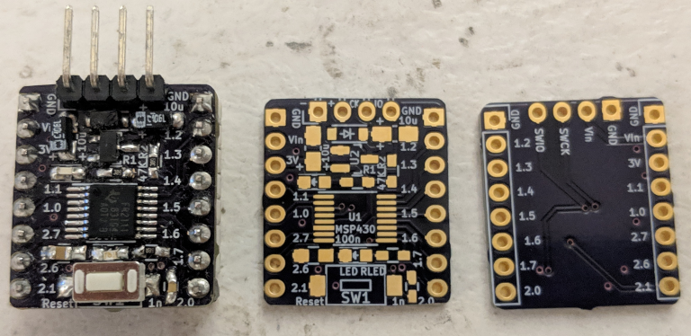
A simple example MSP430FR2111 breakout board design.
I’ll also go over the differences between programming a ‘pulsing LED’ example for the MSP430FR2111 and the MSP430G2553 that we used in the last two examples, as well as how to connect a Launchpad board’s debugger to upload programs to the custom board. So let’s get started!
Hardware Design
It looks like TI provides a basic reference design for their MSP430 chips in the “Applications, Implementations, and Layout” section of each chip’s datasheet. For the MSP430FR2111, it looks like we only need a 10uF/100nF pair of capacitors to decouple the power supply pins, a 47K resistor pulling the reset pin up, and a 1nF capacitor decoupling the reset pin. The reset pin doubles as a data pin in TI’s debugging interface, so they recommend that its decoupling capacitor be <=1.1nF to allow those high-speed signals to work.
I wanted to make this board very simple, so I did not include an external crystal oscillator. I also used a simple 3-pin linear voltage regulator, but a switching buck converter would be a better idea for most of the low-power applications that these chips are designed for. Also, I used a 3V regulator instead of the usual 3.3V, but that shouldn’t make a big difference. So along with a ‘power on’ LED and a test LED attached to P2.1, the overall design looks like this:
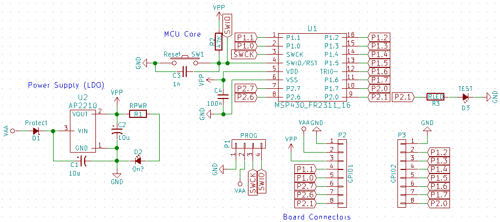
A super-simple MSP430FR2111 Circuit.
Sorry about the incorrect pin markings on the inside of the chip package in that screenshot; I used a part file that I had previously made for an almost (but not quite) identical MSP430FR2311 chip which swaps one of the GPIO pins for a dedicated transimpedance amplifier input. The maroon-colored labels should be correct.
‘Pulsing LED’ Example Code
The MSP430FR2111 is smaller and simpler than the MSP430G2553, so it has fewer peripherals and that includes the timers. Instead of two “Timer A” peripherals, we only have one “Timer B” peripheral available. Its two output channels on CCR1 and CCR2 route to the P1.6/P1.7 pins by default, but that can be changed to P2.0/P2.1 by setting the TBRMP (“Timer B ReMaP”) bit in the SYSCFG3 register. TI’s FRAM chips also protect the GPIO pins from having their state changed until the LOCKLPM5 bit is cleared in the PM5CTL0 register.
But other than that (and the use of TB instead of TA in the timing registers), this code looks very similar to the examples from the MSP430 PWM tutorial; it initializes the LED pin, sets up the timer/interrupt, and then puts the chip to sleep:
#include <msp430.h>

#define MAX_TIME  (1000)
#define MAX_COUNT (20)
int tim = 500;
int tv = -10;
int c = 0;

// Short delay method, until I figure out timers.
void delay (unsigned long int d) {
  unsigned long int i;
  for (i = 0; i < d; ++i) { asm("nop"); }
}

int main() {
  // Stop the watchdog timer.
  WDTCTL  =  (WDTPW + WDTHOLD);
  // Un-lock the GPIO port settings.
  PM5CTL0 &= ~(LOCKLPM5);

  // Set Timer B to use P2 instead of P1.
  SYSCFG3 |= (TBRMP);
  // Setup P2.1 for PWM output.
  P2DIR  |=  (BIT1);
  P2SEL0 |=  (BIT1);
  // Setup Timer 0.
  // CCR0 holds the base PWM frequency.
  TB0CCR0  = (MAX_TIME);
  // Set the 'timer cycle' interrupt to trigger.
  TB0CTL  |= (TBIE);
  // CCR2 holds the duty cycle in 'set/reset' mode.
  TB0CCTL2 = (OUTMOD_7);
  TB0CCR2  = (tim);
  // Start timer 0 to 'count up to CCR0' mode using the system clock.
  TB0CTL  |= (TBSSEL_2 | MC_1);

  // Turn off the CPU, and enable interrupts.
  _BIS_SR((LPM0_bits | GIE));

  // (zzz...)
  while (1) {}
  return 0;
}

__attribute__((interrupt(TIMER0_B1_VECTOR)))
void tim0_b1_isr(void) {
  // Update the colors every N cycles.
  ++c;
  if (c >= MAX_COUNT) {
    tim += tv;
    if (tim > MAX_TIME) {
      tim = MAX_TIME;
      tv = -tv;
    }
    else if (tim < 0) {
      tim = 0;
      tv = -tv;
    }
    TB0CCR2 = (tim);
    c = 0;
  }
  // Acknowledge the interrupt.
  TB0CTL &= ~(TBIFG);
}
Building and Flashing
Since this all fits in one main.c file, we can still use a couple of one-line commands instead of a Makefile to build it:
msp430-elf-gcc -g -Os -Wall -mmcu=msp430fr2111 -I./ -I/usr/local/msp430-elf/include/gcc_include/ -c main.c -o main.o
msp430-elf-gcc main.o -g -mmcu=msp430fr2111 -L/usr/local/msp430-elf/include/gcc_include/ -o main.elf
The extra -I and -L flags tell the compiler and linker where to find the device header files and linker scripts; around the time that TI added support for the newer generation of chips including the MSP430FR2111, it looks like they decided to stop using the msp430mcu project to manage simple ‘glue’ code like linker scripts and device header files. Instead, they now offer a ‘support files’ package which you can download separately, but that also means that you need to tell the toolchain where those files are. You can find a .zip of those files on TI’s MSP430-GCC site, called msp430-gcc-support-files-1.204.zip, and I arbitrarily placed them in a gcc_include folder where the toolchain was installed on my system. Finally, your version of GCC might be called msp430-gcc instead of msp430-elf-gcc.
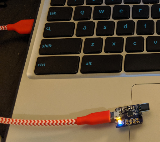
With everything built, you can plug the board into a debugger. On Launchpad boards, the debugger pins are clearly marked; the SBWTCK pin goes to the debugging clock line, the SBWTDIO pin goes to the data line / reset pin, and the power pins connect normally.
Once the binary image is built and the board is plugged in, you can flash it using the same mspdebug steps as before. But since we are using an FRAM device, we don’t need to erase the memory before writing to it like we would with Flash memory. If you include an ‘erase’ command, the newer versions of mspdebug will print a warning reminding you that it is not necessary. So with one of the newer boards using a tilib debugger:
mspdebug tilib 'load main.elf' 'exit'
And once the program is uploaded, the on-board LED starts pulsing.
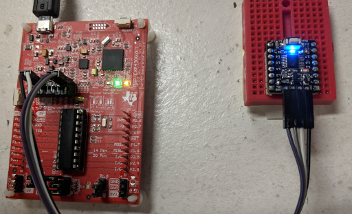
MSP430FR2111 board connected to a Launchpad debugger.
Conclusions
It turns out that programming an FRAM device is just like programming a regular device, and it is pretty easy to design and program a custom MSP430 board. I guess that the applications of nonvolatile RAM are sort of limited because of its cost and low storage density, but it certainly seems more flexible than Flash memory.