
It’s great to be able to write programs for a chip’s evaluation boards, but the real strength of microcontrollers is their ability to act as a low-cost, low-power “brain” for larger designs or products. And along those lines, I’ve been writing a few tutorials about bootstrapping some basic ‘bare metal’ STM32 projects using an STM32F031K6 “Nucleo” board sold by ST.
That’s a great way to get started and test ideas out, but what if you want to try your hand at building a robot, or a home automation widget, or some other sort of complex machine? It’s nice to avoid huge messes of breadboards and wires once you have a basic prototype working, and these days it only costs a few dollars to get a small custom circuit board manufactured. The catch is, they usually take a few weeks to arrive and you need to provide the design. Still, the boards that we design in this tutorial will cost less than $2 each.
In this tutorial, we will use a suite of free software called KiCAD to produce a small example board using the same basic STM32F031K6 chip that I’ve been writing programming examples for. Our board won’t be quite as nice as ST’s, and it will require an external USB device for programming and debugging. But on the other hand, our board will be smaller and cheaper, and you will be able to put the same design onto more holistic boards with other parts for your kickass robot or electronic vehicle or <insert dream here>:
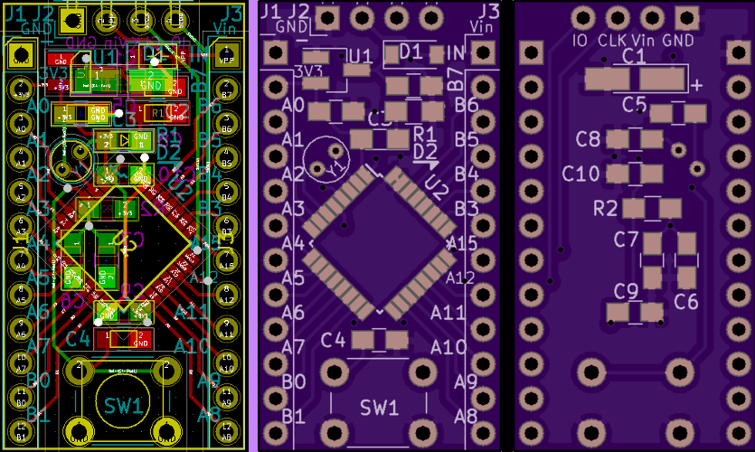
Left: A board like the one you’ll design in KiCAD. Right: OSHPark’s renders of the front and rear of the board.
The design files described in this post are all available in a Github repository, if you want a reference to follow along with.
KiCAD
KiCAD is a free and open-source suite of “EDA” (Electronic Design Automation) programs. You can download and install the whole thing from their website; your package manager might also have it available, but that could be an old version and KiCAD has improved a lot over the past couple of years. It has matured into an accessible and powerful tool, and it is still under very active development with the occasional new feature being added. You may also have to install a “KiCAD Extras” package to use the default libraries and footprints.
The process of designing a board in KiCAD typically follows these general steps – I’ll try to describe each one briefly before we get started:
Schematic Capture
The first step in designing a printed circuit board is defining the abstract circuit that we want to lay down on the board. If you’ve worked with electronics before, you will probably be familiar with the way that schematics are used to describe an electronic circuit. If not, here is a quick overview. In a program like KiCAD, we will define our schematic by placing each part on a grid, and then linking those parts’ connectors together with wires drawn on the same grid.
Part Design
If KiCAD does not have a schematic file available for one of our parts, we can create one. This is often necessary if you use integrated circuits, because there are just too many chips available to keep up-to-date entries for all of them in the default libraries. Would you want that job? I wouldn’t.
Linking Schematic Parts to “Footprints”
Once we have a complete abstract circuit, we need to tell KiCAD what each part will look like in the real world. The shape and size of a part will determine what its “footprint” should look like on the circuit board; we want to expose copper on the board at the places where we want to solder parts on, so it is important that those copper pads and holes are correctly placed depending on the size of each part.
Footprint Design
Similar to the abstract schematic parts, if KiCAD does not have a “footprint” file available for a physical part, we can create one. This step will not be necessary in this tutorial and I will be skipping it to keep things simple, but it is useful if you need to use oddly-shaped parts.
PCB Layout
Finally, the last step is to import the combined schematic and “footprint” data onto a grid which is measured in physical units like inches or millimeters. Each part will be represented by the physical “footprint” that you assigned to it, and the pads on those footprints will have lines drawn between them to highlight connections which still need to be made between parts.
So all you have to do is draw a physical outline for the board, place the parts within that outline, and then draw the appropriate connections between them. Once you get to this step, it’s like playing a puzzle game. KiCAD includes a design-checking feature too, which double-checks the schematic against the physical board and tells you if anything anything is incorrectly connected (or disconnected) before you send the board off to be manufactured.
Minimal ‘STM32F031K6’ Circuit
Starting KiCAD
When you first start KiCAD, it will open a “project overview” window. This window is mostly for organization; it shows your project’s files on the left sidebar, and has several large buttons to open new windows for each major step in the KiCAD workflow:
KiCAD starting screen
Starting a New Project
We can’t open any of the circuit design tools until we create or open a project; the icons are grayed-out. So, click the ‘Create New Project’ button:
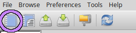
“New Project” button, circled in lavender.
In the file browser that opens up, pick a folder to hold your project, enter a name, and hit ‘Save’.
Before we get started with the actual tools, a mild word of warning: KiCAD uses keyboard commands instead of mouse clicks for a lot of common operations, so the primary mouse button might not always do what you expect. One example is moving parts; instead of clicking on a part to ‘pick it up’, you need to move the mouse over it and hit m (for ‘Move’) on the keyboard. I will call out all of the keyboard shortcuts used throughout this tutorial, but you should be aware of that quirk.
On the bright side, you can press the ? key in most windows to bring up a quick list of hotkeys that will work in the current tool. If you accidentally press a random key and something weird happens, that can be a useful safety net. Also, pressing the escape key will usually cancel the currently-selected tool.
Making a Part File
The first tool we will use is the ‘Part Library Editor’; before we design a circuit around the STM32F031K6, we need to tell KiCAD how many connections the chip has, and what each connection is called. KiCAD does already have a physical footprint for the chip, since ST used a common standard size: we’re looking at a 7x7mm QFP32 chip, which means “Quad Flat Package with 32 pins”.
The “Quad Flat Package” is a common and recognizable shape; you might have seen them before if you’ve looked at bare circuit boards before:
A random QFP32 chip in its natural environment; from a Wikipedia page, because they use royalty-free images.
But what does each of the chip’s 32 pins do? And how should we connect each one to our circuit?
Gathering Required Information
Basic information like pin definitions and physical footprint dimensions can usually be found in your chip’s datasheet. In this case, Section 4 has pictures with the “pin-out” of each chip, and a table later in the datasheet describes each of those pin’s names and functions in more detail. The 32-pin QFP chip looks like this:
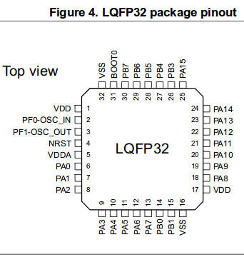
Pin definitions for the STM32F031K6
The pins marked VDD should be connected to the positive voltage supply, and those marked VSS should connect to ground. VDDA is an analog voltage supply pin; adding extra filtering to that pin can reduce noise on the chip’s analog peripherals. And the pins marked PAx, PBx, PCx, etc. are GPIO (“General-Purpose Input/Output”) pins. For example, PA2 is connected to the ‘pin 2’ settings in the GPIOA registers.
Creating a New Part
In KiCAD, the process for creating a new part is pretty simple. For the STM32F031K6, we only need to place 32 pins and assign a label and pin number to each one. Later, when we assign a 32-pad physical footprint to this 32-pin schematic part, pins and pads with the same number will be linked. You can also draw shapes and text, to visually identify the part in the schematic view.
Optionally, you can also set a ‘type’ for each pin (power supply, input/output, etc) if you want KiCAD to run design checks on your schematic. But I will not cover that in this tutorial, for the sake of simplicity and because I haven’t quite figured it out yet.
So let’s start by opening the ‘Part Library Editor’ tool – that is one of the large buttons in the “project overview” window:
KiCAD’s “Part Libary Editor” button
When we click on that icon, a new window will open, looking something like this:
KiCAD’s “Part Library Editor” tool, with no library or part selected.
The large grid view is where we will lay out the pins and draw an outline; when the part is added to a schematic, it will show up as we draw things in this view. So the first step is to click the ‘Create a New Component’ button, and enter a name:
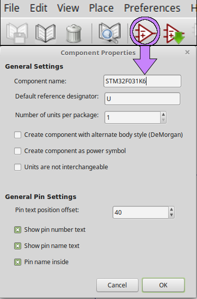
To create the STM32 part, click the circled button on the top bar, enter a name, and click ‘OK’.
Lifting Labels, Placing Pins
Great, now there is an ugly jumble of letters in the middle of the view. The part’s name and reference start on top of each other at coordinates (0, 0). Every part in a circuit schematic has a reference ID which contains a ‘designation’ and a number. The number typically counts up from 1, while the designator describes the part in broad terms. For example, ‘R’ means ‘Resistor’, ‘C’ means ‘Capacitor’, ‘D’ means ‘Diode’, and ‘U’ means ‘Integrated Circuit’.
To move these labels around, you can move your mouse cursor over them and hit the m key. If there is only one thing underneath the cursor, it will be picked up. But if there are multiple options, a ‘Clarify Selection’ menu will pop up under the mouse cursor, and you can select what you want to move. Once a part is picked up, the enter key or primary mouse button places it back down, but pressing m again will not:
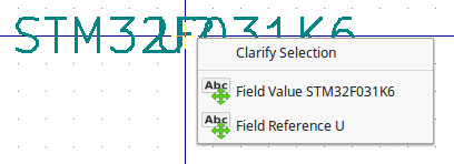
The “Clarify Selection” dialog menu.
That’s just one of those ‘keyboard quirks’ that I mentioned earlier. This is also a good time to mention that you often don’t have to use the mouse at all in KiCAD’s various grid-based tools; the arrow keys will move the grid’s cursor one step at a time, and hitting enter often does the same thing as clicking the mouse button. So to move a label a couple of grid ‘ticks’ up, you can just hit m, up, up, enter. You can also use the arrow keys and enter to select options in the “Clarify Selection” dropdown menu. If you like shell prompts, you’ll probably like KiCAD.
Anyways, once you have the labels arranged, you can either click the ‘Add Pins to Component’ button on the right sidebar and then click somewhere in the grid view, or hit the p key to place a new pin:
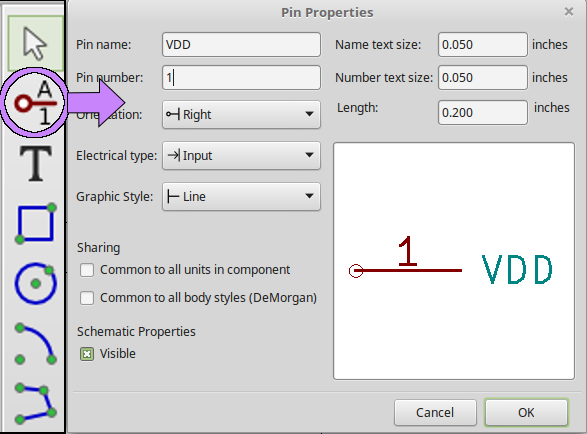
Adding a pin to a part – the “Add Pin” button is on the right sidebar.
Then, you can just lay out the pins one by one, referring to the datasheet’s “Pinout” definitions described above. To rotate a pin, press the r button either after picking it up with m, or with the cursor hovering over it:
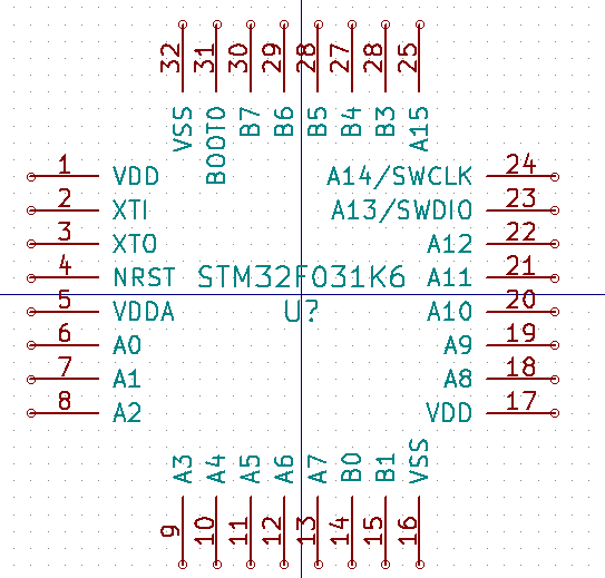
All 32 pins added, in a square pattern.
Are you grimacing right now? I think that most experienced designers would tell you that this is a bad way to lay out a schematic part, and they would probably be right. It seems like most engineers lay out chips with pins grouped in rows based on their functions, instead of their actual location on the part. A schematic does not need to visually resemble the final circuit on the board. Its main purpose should be to make the circuit easy to understand at a glance.
But this is a simple part, and I like being able to lay out schematic components while thinking about how they might fit on a board. It doesn’t really matter too much unless you have to deal with a lot of pins, anyways. You can draw shapes with the buttons on the right sidebar; I’ll add a rectangle around the general area by clicking the ‘Add Rectangle’ button. With a ‘draw’ tool selected, pressing enter or clicking the primary mouse button both starts and finishes the shape – with rectangles, the “start/end” clicks define two corners:
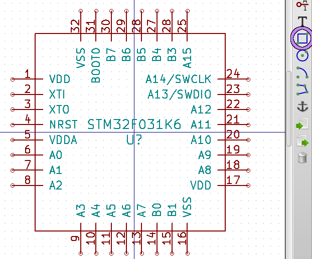
Finished STM32F031K6 part. The right sidebar’s “Draw Rectangle” button is circled in lavender.
When you draw “Line” shapes, you may need to right click and select the “End Drawing” option to stop drawing new segments. But that’s it, our STM32 part is now finished!
Did you notice that I accidentally marked pin 26 as pin 28? I didn’t, until I got halfway through laying out the PCB. Be careful about that sort of thing 🙂
Saving the Part
If you haven’t made custom parts in KiCAD before, you will need to create a new “library” to save the part in. KiCAD schematic libraries are stored in .lib files, which you can copy across machines and easily import into other installations of KiCAD. So, click the ‘Save Current Component to New Library’ button, choose where to save the .lib file, and hit ‘Save’:

The “Save to New Library” button
You’ll probably get a message saying, “This library will not be available until it is loaded by Eeschema”. You need to import libraries to use the parts saved in them, and you can do that from either this ‘Part Library Editor’ tool, or the ‘Eeschema’ schematic design tool which we will go over next. In either tool, you can click on the Preferences -> Component Libraries menu, and then click the large ‘Add’ button to select a library file to import:
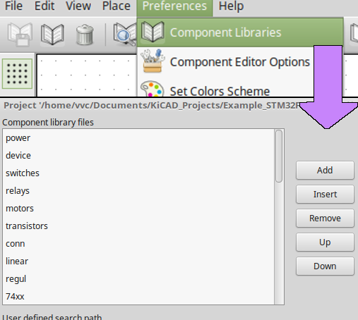
Adding a part library to a project – the “Add” button opens a file browser.
Click ‘Okay’ to close the ‘import library’ window. Finally, to save our part, we need to set a ‘current library’ to tell KiCAD which library it should save to when we hit ctrl+S. This can be done with the ‘Select Working Library’ button, which will open up a list of default and imported libraries for you to pick from:
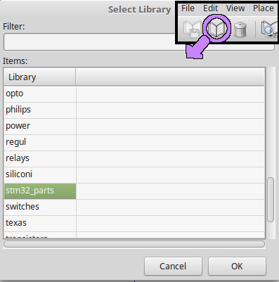
Selecting a “Current Library” – the “Set Current Library” menu button is highlighted in lavender.
With a “Current Library” selected, if you make any more changes to the part, you can save them with Ctrl+S or from the File menu. Click ‘Yes’ on the confirmation menus to update the part in the library.
Kind of a complicated process for just saving a file, huh? But you don’t have to do it very often, and now we can move on to the actual circuit schematic. You can close the ‘Part Library Editor’ window once you’ve saved the STM32F031K6 part in a library and imported the library into your project. If you get a warning that your changes still need to be saved and the File -> Save Current Library option does not work, review the above steps and make sure that the part is saved in your custom library before continuing.
Designing a Minimal Circuit
The basic steps for designing a board for the STM32F031K6 are described in ST’s “Application Note 4080,” titled “Getting started with STM32F0x1/x2/x8 hardware development”. Here is the minimal circuit that we will produce in the following sections; I hope that it implements most of the guidelines presented in that document:
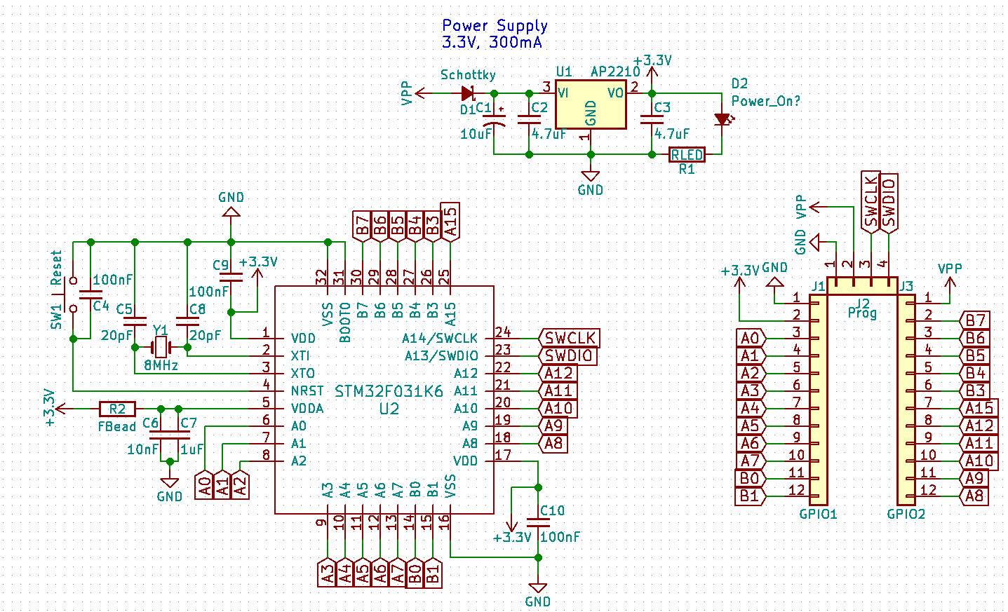
A basic STM32 schematic
Let’s look over each part of this circuit, and how to construct it. Open the ‘Eeschema’ tool by clicking on its large icon in the ‘Project Overview’ window, and then we’ll start with the power supply:
The button for opening KiCAD’s circuit schematic tool, called “Eeschema”.
3.3V Power Supply
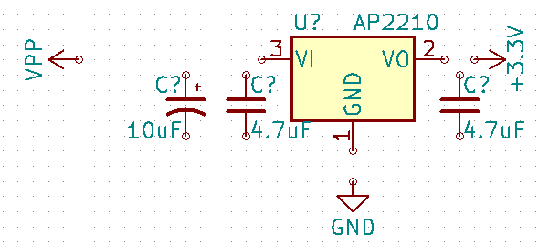
To make sure that the correct voltage is provided to our microcontroller, I used a simple +3.3V linear voltage regulator, specifically an AP2210-3.3 which can provide 300mA of current. I chose it because it is a small, cheap, and simple regulator with only 3 pins – Input, Output, and Ground. It should work for input voltages between roughly 4-12V, which should be fine for this minimal design; the USB port on your computer typically provides +5V.
The AP2210 lists an example “reference circuit” in its datasheet, and that recommends placing one capacitor between Ground and each of the ‘Voltage Input’ (VI) and ‘Voltage Output’ (VO) pins. Reference designs are typically good starting points, but the datasheet also points out that capacitors with larger capacitance values should help the regulator provide more stable output voltages, so it is not a bad idea to use larger capacitors than the ones shown.
Instead of making a new part for the AP2210, we can use an existing 3-pin voltage regulator in KiCAD’s default library. To find one, press the a key (“Add Part”). A window will pop up with a list of libraries, and a search field. Entering, “Regulator” into the search field brings up a few options, and it looks like the common (but higher-power) AP1117 has the same VIN/VOUT/GND pin numbers – we can just re-name it:
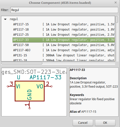
Meh, close enough.
So select the AP1117, click ‘Okay’, and then click anywhere on the grid to place the part. We’re going to use an AP2210 as mentioned above, so hit the e key with your cursor over the label that reads, “AP1117”. The ‘Edit Label’ dialog lets you change the label’s text, size, alignment, etc. For now, just change it from “AP1117” to “AP2210”:
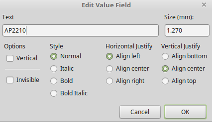
The “Edit Label” dialog box
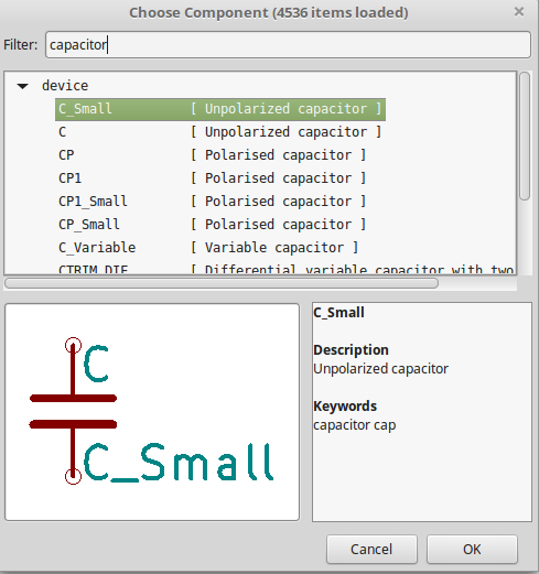
The datasheet’s reference design recommends a 1uF ceramic capacitor on the input, and 2.2uF on the output. Larger values should further stabilize the output though, so I’ll use slightly larger values. It is also a good idea to place either an electrolytic or tantalum capacitor across the main power input line. Those “chemical capacitors” have different properties from ceramic ones, and they reduce noise and interference at different frequency ranges. You can add capacitors just like you added the voltage regulator; press the a key, enter “Capacitor” into the filter field, and select the type you want:
Adding a simple capacitor part
‘Polarized Capacitors’ represent capacitors made of things like tantalum or aluminum chemistries. You need to connect their anodes (‘flat’ side) to a positive voltage, and their cathodes (’rounded’ side) to a lower voltage or ground. “Unpolarized Capacitors” represent those made of things like ceramics, mica, PTFE films, etc. You can connect them in either direction.
So, try placing a few capacitors around the regulator and editing their labels to show the desired capacitance values – remember, a adds new parts, m moves them, and e edits them. You can also “flip” a part across its X or Y axis with the x or y key, and rotate it by 90 degrees with the r key:
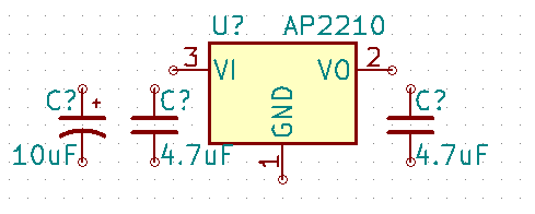
Adding a few capacitors to the regulator
Next, we need to add “power” labels to tell KiCAD which power lines each of the regulator’s pins will connect to. To add a power label, hit the p key. There are several default labels for various common voltages and grounds, and it works exactly like adding a new part. I will use +3.3V for the output line, GND for ground, and VPP for input power:
Adding power labels to the voltage regulator circuit
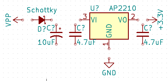
You can move and rotate power labels just like parts, with the m and r keys. We should also add a schottky diode between the VPP input voltage and the regulator; doing so will protect your board from damage if you accidentally apply power with reverse polarity. A schottky diode is used because its low forward voltage will let the regulator continue working with a lower minimum voltage than an ordinary diode would. Typing ‘schottky’ into the ‘filter’ field will get you the appropriate schematic part. Make sure that the diode is pointing in the right direction:
Regulator circuit with a protection diode added
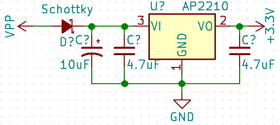
To connect everything together, you only need to draw ‘wires’ between the open circles on each schematic connection. Press w to start drawing a wire under the mouse cursor, and move the mouse to ‘drag’ the wire’s potential path. When you click the mouse button or press w again, it will place a ‘corner’ and you can continue drawing the wire in a different direction. When a ‘corner’ is placed on the same grid coordinate as an existing wire or a part connection, the wire will automatically connect to that and finish. You can also press escape to cancel drawing a wire partway through, or right click and select the “End Wire” option to stop the wire at the current grid coordinate. When wires cross, they will have a filled-in circle over the junction if and only if the wires actually connect to each other. This is important, because it is a common cause of confusing errors – if there is no circle over two crossed wires, those wires are not connected in the schematic! Keeping that in mind, try drawing some wires to connect the regulator, capacitors, diode, and power lines:
Power supply with all of the parts connected
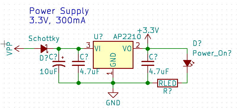
I also like to add an LED to the +3.3V output, so that people can quickly tell when the board is powered on. This is optional, but you can add an LED and resistor (about 4.7KΩ or so) using the same steps as above. Also, you can press the t key to add text to the schematic, so I labeled for this area as the power supply:
Power supply circuit with text label
Finally, when you finish a ‘block’ of a larger circuit, it is usually a good idea to click the ‘Annotate Schematic Components’ button to automatically assign a number to each part that doesn’t already have one. All of those symbols like C? and U? will have their ?s replaced with an ID number. Click ‘Okay’ if you get asked for confirmation after clicking the ‘Annotate’ button:
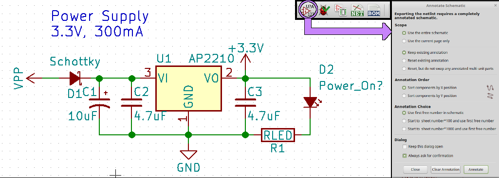
Finished power supply circuit with auto-numbered parts
That’s all we need for the power supply! Now, on to the actual STM32 microcontroller.
Placing the Microcontroller
The STM32F031K6 is the core of this circuit – with the custom part created and our custom library imported into the project from the previous steps, you can add it like any other part with the a key – just enter ‘STM32’ in the ‘Filter’ field, and the part should come up:
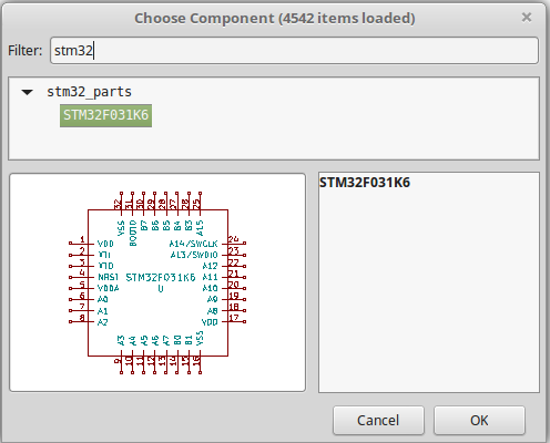
Adding the STM32 schematic part
If the part doesn’t appear in the ‘Add Part’ menu, that probably means that either your custom library is not imported, or your custom part has not yet been saved into the library.
Decoupling and Filtering Capacitors
The STM32 line of chips require some “decoupling capacitors” placed between the part’s power pins, and ST also recommends adding a couple of extra filtering capacitors to the ‘Analog Voltage’ pin. Again, these capacitors should improve the stability of the chip’s power supplies.
I also added a ferrite bead between the 3.3V supply and the ‘Analog Voltage’ pin, as an extra measure for reducing high-frequency noise to hopefully improve the accuracy of the chip’s ‘Analog/Digital Converter’ pins. For that, I used the same schematic symbol as a resistor; close enough.
There are two pairs of VDD/VSS pins on the STM32F031K6; place an unpolarized capacitor between each one, along with the analog filtering parts described above:
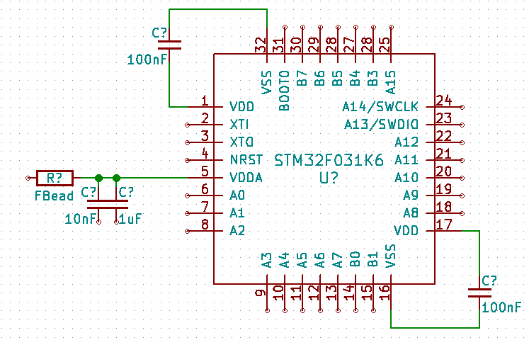
A few recommended “decoupling capacitors”, plus an optional ferrite bead for the analog supply.
For power, the VDD pins should connect to +3.3V, and the VSS pins should connect to ground. The VDDA pin should connect to +3.3V through the ferrite bead (if you’re using one), and the other side of its capacitors should connect to ground. So, also place and connect those power labels:
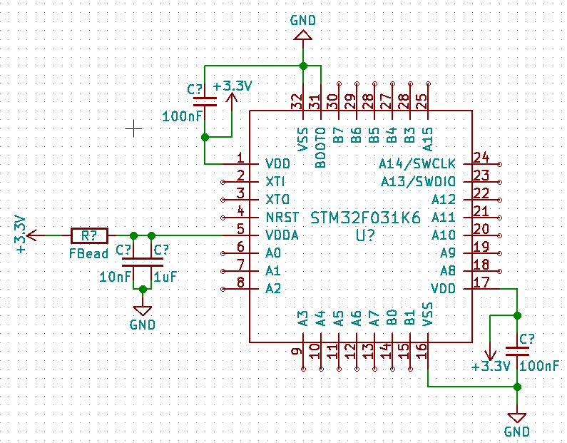
Add power and ground labels to connect the chip to the power supply.
The BOOT0 pin is also connected to ground. If it is left floating, the chip will not know where to boot from when it starts up. If it is pulled to +3.3V, the chip will not boot from its core flash memory, and that is a fairly advanced feature which most starting projects do not use. It also seems like a common source of problems for new designers, so I recommend just connecting the pin to ground for a basic board.
8MHz Crystal Oscillator
While the STM32 line of chips does include an internal 8MHz RC oscillator, its frequency is not very stable over changing temperatures, voltages, etc. Code which depends on very precise timings may not function consistently across Earth’s myriad biomes. Adding an external crystal oscillator with a precise 8MHz frequency lets us give the chip a more accurate core clock signal which is good enough for most “realtime” applications. It should connect to the STM32’s OSC_IN and OSC_OUT pins, and 20pF capacitors are connected between each side of the crystal and ground per the application note’s recommendations:
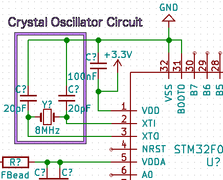
Crystal oscillator circuit connected to the STM32
“Crystal” is often abbreviated as “XTal”, so I used XTI and XTO as labels for the STM32’s external oscillator input/output pins, and I used one of KiCAD’s built-in ‘crystal’ schematic parts. This is technically optional, though; you don’t need an external crystal oscillator.
Reset Button
The ‘Reset’ button is connected to the NRST pin – when the pin is pulled low, the system resets. The STM32 lines include a pull-up resistor internally connected to the reset pin, so we don’t need to include one on the board. The datasheet does recommend a 100nF capacitor in parallel with the button, though:
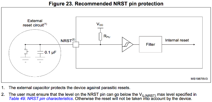
ST’s recommended “reset button” circuit, copied from the datasheet
With one side connected to ground and the other connected to the reset pin, pressing the button will reboot the system. KiCAD also has built-in schematic parts for ‘push-button’ switches – enter “push” in the ‘filter’ field of the “Add Part” dialog box if you’re having trouble finding them:
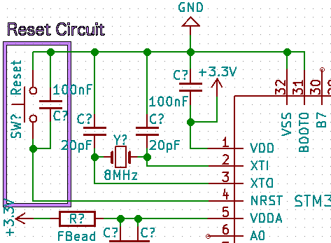
The simple “Reset Button” circuit
Pin Connectors
Besides the circuit parts, it’s a good idea to connect the chip’s GPIO pins to an external connector like breadboard pins. We’ll also need a way to provide power, and it’s nice to have a few power output connectors as well since there’s already a voltage regulator on the board. Also, you’ll need a few connections for programming the chip.
A good way to do this in KiCAD is to add parts from the default conn (“Connectors”) library – they are simple rows of open connections in the schematic, and KiCAD comes with physical footprints to place plated holes at the 0.1″ spacing of common breadboards.
In this example, I will use one CONN_01x04 part for programming the chip, and two CONN_01x12 parts for rows of pins which can plug into a breadboard. For the GPIO pins, it’s a good idea to use labels to connect them – otherwise, you can wind up with a spaghetti mess of wires. To place a new label, press Ctrl+H or press the ‘Create Global Label’ button. You can then connect a wire to it like a normal part:
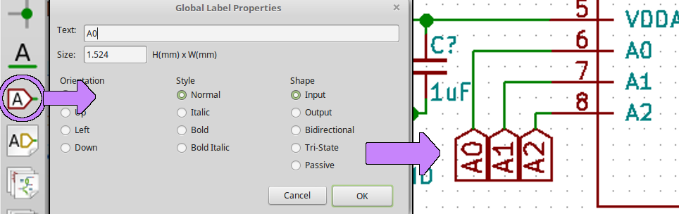
Creating schematic labels
The A13 and A14 pins are a special case – they can be configured as normal GPIO pins, but they are also used to program the chip, so I am going to connect them to a separate connector. A13 is the SWDIO (“Debugging Input/Output”) pin, and A14 is the SWCLK (“Debugging Clock”) pin. A full JTAG interface is also supported, but you only need those two pins.
So, here is what I wound up with. Labels with the same name will be connected to each other, so the connections in the following image will wire the GPIO pins and power lines to two rows of connectors, and the programming pins to a separate connection which also has power input pins:
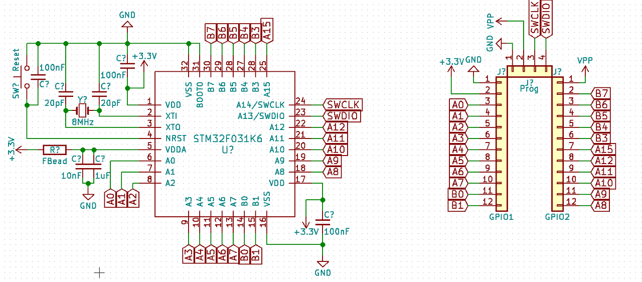
The rest of the labels, with “pin headers” connected to them.
Linking Footprints to the Schematic
Great, our circuit schematic is complete! All of the STM32 pins are connected, and the power supply will provide the chip with an appropriate voltage. But before we can lay out a circuit board, we need to tell KiCAD what each part looks like in the real world. To do this, click on the ‘Associate Components and Footprints’ button. If any parts still have a ? instead of an ID number, the same ‘Annotate Components’ view that we used to number the power supply components will open. You can click ‘Annotate’ again to fill in any missing numbers like before, and click ‘Okay’ if it asks for confirmation:

The “Associate Components and Footprints” button
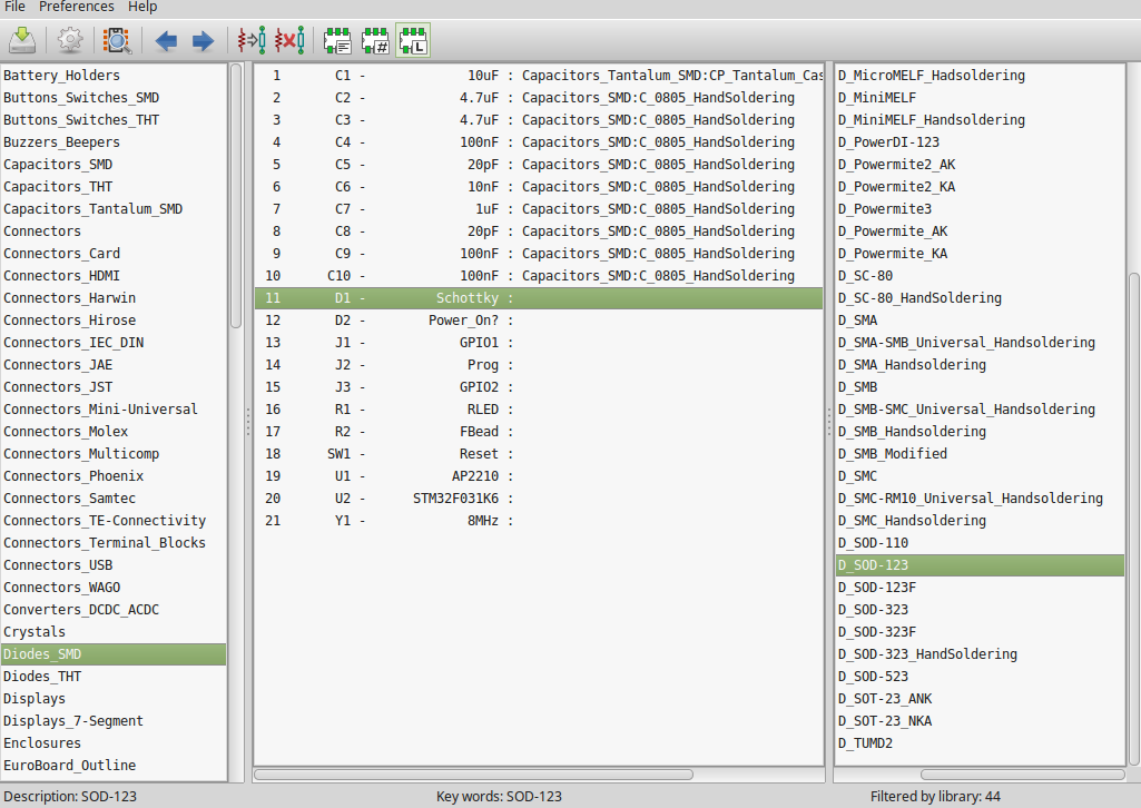
This opens a new tool called CvPcb – its interface has three major columns. On the left are the footprint libraries that you can select from. In the middle is a list of the parts on your board. And on the right is a list of available footprints in whatever library is currently selected in the left-most column.
KiCAD offers different ways to filter footprints, and a filter based on the part keywords is often enabled by default. It can be useful, but I usually find it easier to turn that filter off so that no footprints are hidden; in the top menu bar, I recommend making sure that only the rightmost ‘Filter Footprint List by Library’ button is selected:
The filter options are circled in lavender; this tutorial assumes that only the rightmost “L” (“Library”) filter is selected.
The footprint libraries’ names generally do a good job of describing what sort of parts they contain. For capacitor footprints, click on one of the ‘Capacitors’ library:
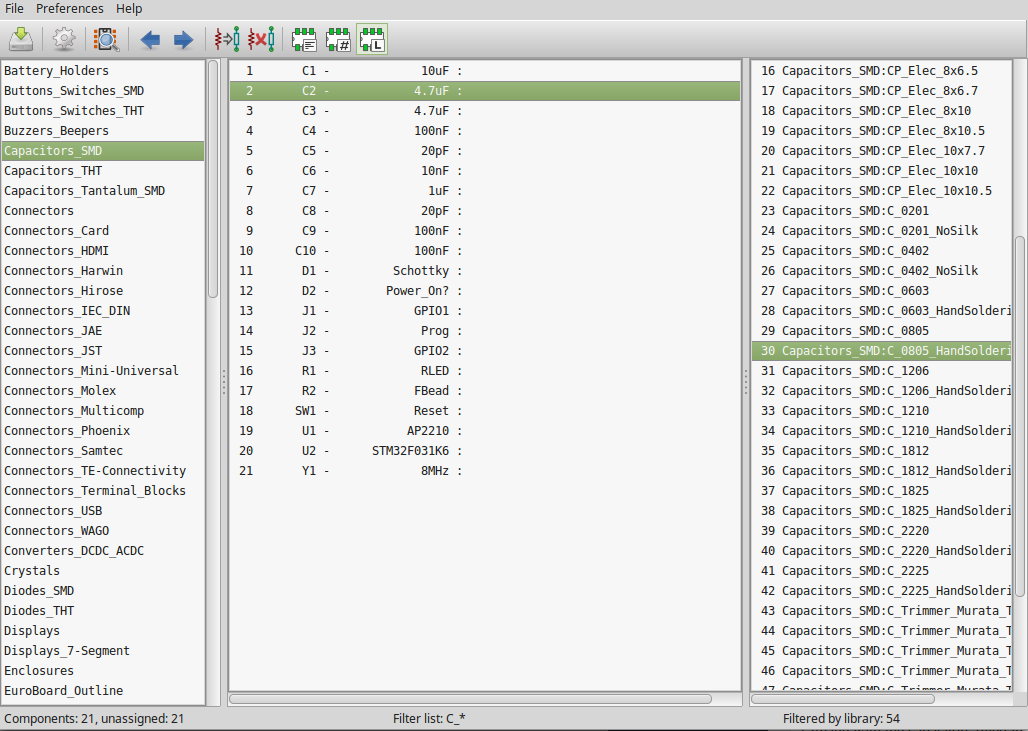
The main “CvPcb” view, with the “Capacitors_SMD” library selected.
I’ll be using surface-mount components, so I’ll use the ‘Capacitors_SMD’ library. If you want to use through-hole passives, you could use the ‘Capacitors_THT’ library instead. The C1 10uF capacitor is polarized, so I’ll use a part from the ‘Capacitors_Tantalum_SMD’ library for that one with a common Size A footprint (aka 3216 or 1206):
Footprints assigned to the capacitor parts.
For the ceramic capacitors, 0805 is a common size, and large enough that it is easy to solder by hand. The footprints which end in _HandSoldering have extra-large pads, which make it nice and easy to assemble without a reflow oven. I will link to example parts that you can buy for all of these footprints at the end of the post in a ‘Bill of Materials’ section. I’ll use an SOD-123-sized schottky diode, and a 3mm-diameter cylindrical crystal oscillator. These are common sizes and again, you can find example parts at the end of this post.
Footprints for the row connectors can be found in the ‘Pin Headers’ and ‘Socket Strip’ libraries; most 0.1″ pin headers should fit. If there are multiple sizes, the 2.54mm ones should work with a breadboard. The voltage regulator’s SOT-23 package can be found in the ‘TO_SOT_Packages_SMD’ library, and the QFP32_7x7mm footprint for the STM32F031K6 is under the ‘Housings_QFP’ library. For the reset button, the through-hole SW_PUSH_SMALL footprint seems to fit the ubiquitous ~6mm tactile push-buttons. More recent versions might have a SW_PUSH_6mm footprint instead. And I used 0805-sized parts for everything else:
The “Part / Footprint” associations that I wound up using.
Once every part has a footprint, you can click File -> Save Edits and close the tool. If you are using a different version of KiCAD, the default footprints may have slightly different names.
Generating a Netlist
Finally, we just need a “Netlist” file which contains the schematic information along with footprint associations, and can be read by KiCAD’s PCB design tool. This is a quick step – just click the ‘Generate Netlist’ button in the schematic view, click ‘Generate’ in the dialog that comes up, and then click ‘Save’:
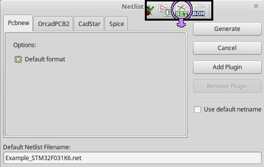
KiCAD Netlist generation dialog – just click ‘Generate’ and save. The default netlist filename should work fine.
Now for the fun part, designing the circuit board!
Laying Out the Circuit Board
Importing the Parts
To use KiCAD’s ‘PCBnew’ tool, click on its icon in the ‘Project Overview’ window:
The “PCBnew” tool’s icon
You’ll be presented with an empty grid, just like when you first opened the schematic editor. To import our circuit, all you have to do is click the ‘Read Netlist’ button, click ‘Read Current Netlist’, and then ‘Close’. If you make changes to the schematic later on and want them to be reflected on your circuit board, you can simply re-import a slightly different Netlist, and change the options for things like “Exchange Footprint” and “Extra Footprints” to tell the importer how to handle mismatched parts:
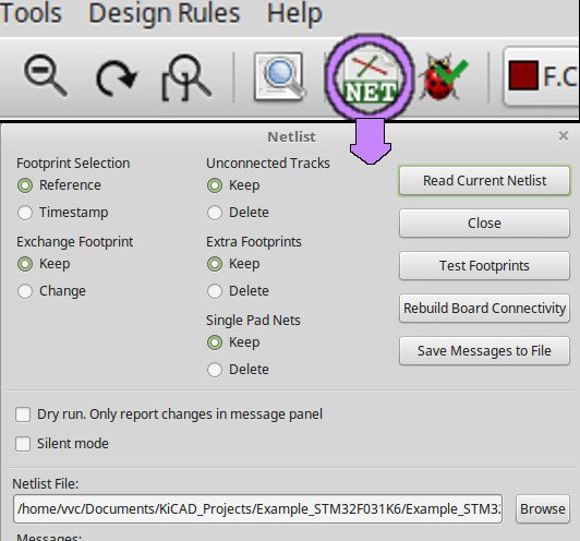
Reading the Netlist
All of the parts are placed on top of each other at the grid’s origin by default, which can be bewildering to look at. You can spread them out by clicking the ‘Automatic Footprint Placement Mode’ button, right clicking in the view, and selecting Global Spread and Place -> Spread All Footprints:
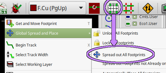
Automatically spreading the part footprints – remember to de-select the button on the top menu afterwards!
You can also manually move all of the parts with the m key, just like in the schematic view. If you do auto-move the parts, don’t forget to de-select the ‘Automatic Footprint Placement Mode’ once you are done; it can cause some confusing options to appear, and it changes the meanings of some common hotkeys like e. With all of the parts placed apart, you can see that thin white lines connect the pins that we wired together in the schematic – if any connections look like they are missing, double-check your schematic and label names:
The parts shown in the ‘PCBnew’ tool
Outlining the Boards
It’s usually a good idea to start with the general size of your board, although if you aren’t careful you can design yourself into a corner by trying to make a board too small. But for a simple design like this, let’s just move the two long rows of pin headers 0.6″ apart with the STM32 in between them, place the programming pins along the ‘top’ of the board, and draw a border around those parts. The 0.6″ spacing seems to work with most breadboards, although I’ve found that 0.575″ can fit a bit better.
The grid’s scale is shown in the Grid: dropdown menu along the top of the window; it is shown in both millimeters and “mils” which is a confusing name for 1/1000 of an inch. You can make the grid one step smaller with the n key, and one step larger with Shift+n. 0.6″ is 600 mils, so let’s set the grid to 100 mils and place the connectors 6 grid cells apart. You can use the same hotkeys as in the schematic view; m moves footprints, and r rotates them:
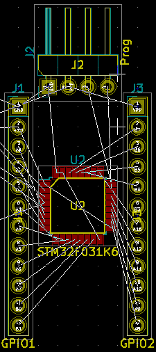
The general board outline – it’s a bit small, but there’s enough space.
Placing the chip perpendicular to the pins like that is a bit awkward, so let’s rotate it by 45 degrees; press the e key while your mouse is over the chip to open its “Edit Properties” window, and in the left panel under the “Rotation” box, select “Other”. These angles are measured in tenths of a degree, so enter -450 in the “Rotation” text box, and then click “OK”:
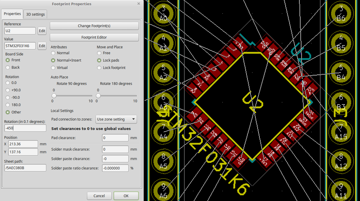
Rotating the STM32 chip by 45 degrees
Looking good! Now let’s draw an outline around those parts. KiCAD’s “PCBnew” tool lets us interact with one of the circuit board’s individual “layers” at a time. Each layer has a color on the grid. The most important layers are:
- “Copper” layers, which represent areas of the board which should have plated copper covering them. The top copper layer is red, and the bottom copper layer is green. When an area is covered by both copper layers, it has a gold color (“red + green”).
- “Silkscreen” layers, which represent areas of the board that should have legible ink covering them. These are usually the layers you’ll put words and symbols on, so that people can read them. The top silkscreen layer is blue, and the bottom silkscreen layer is purple.
- “Fabrication” layers, which you can see in KiCAD but which will not show up on the manufactured board. Part names are placed on the fabrication layer by default. The top fabrication layer is yellow, and the bottom fabrication layer is red.
- The “Edge Cuts” layer, which defines the edges of the board. When you draw a closed shape on this layer, everything inside of that shape is considered to be part of the board. There is only one “Edge Cuts” layer, and it is yellow.
So to outline the board, we should draw some lines on the “Edge Cuts” layer. Click on the Edge.Cuts label in the right-most panel, and then select the “Draw Line” option. Click on the grid space in one corner of the board to start drawing, and place lines around all of the parts. You might want to drop the grid down to 50 or 25 mils, to get the board edges closer to the pins. When you are done, press the escape key or right-click and select the “End Drawing” option:
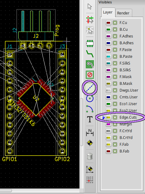
The board with a rectangular outline
Placing the Footprints
Next, we need to move the rest of the footprints onto the board in orientations that will let us easily connect the correct parts by drawing on the copper layers. Basically, you want to put pads which are connected by the thin white ‘guide’ lines as close to each other as possible, and you generally want to avoid having big jumbles of intersecting lines when possible. For placing small parts, I often use a smaller grid size such as 5 mils.
I’ve found that it is helpful to place all of the parts before starting to connect them, in case you have to move things around to get an unexpected part to fit. Again, the same “movement” hotkeys can be used here as in the schematic editor; m moves a part, r rotates it, and e edits its properties. You can also use the f key to “flip” a part to the other side of the board; I ended up putting the tantalum capacitor on the rear, which is the green part in the image below.
So, let’s start by placing the power supply components near the power pins at the ‘top’ of the board. I also moved the labels around a bit so that the “Fabrication” layers are outside the board:
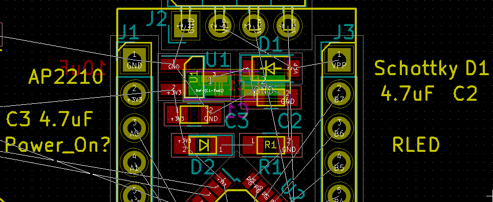
Power supply footprints
You can see that I placed the capacitors close to the regulator pins that they connect to, and the resistor/LED are rotated to minimize the distance between their connected pads. This is important, because adding more than 2 copper layers is expensive and it’s usually best to keep the copper wires – called “traces” – as short as possible.
Anyways, that just leaves the STM32’s supporting circuitry. I put the capacitors on the bottom side of the board, the crystal near the oscillator pins, and the reset button just ‘below’ the STM32. It could be prettier – I like to leave room for including the part values on the silkscreen instead of leaving them off the board – but this is just an example layout:
Footprints all placed on the board
Drawing the Copper Layers
Now for the part that makes this a circuit board; we need to make sure that all of the pins connected by ‘guide’ lines will be connected by conductive copper in the real world. To improve the stability of the board’s signals, it is usually a good practice to place large planes of copper in areas where there aren’t any traces. Usually, those planes are connected to ground, but you might also want to draw these copper “pours” for things like high-power connections.
KiCAD makes this very easy – all we have to do is draw an outline around the area that we want to fill with copper, and it will update the filled areas as we draw traces to make sure that they don’t intersect. Click on the “Add Filled Zones” button with the F. Cu (“Front Copper”) or B. Cu (“Back Copper”) layer selected, choose the power label that you used for Ground, and then draw the outline just like the “Edge Cuts” lines – once you’re done, right click and select “Close Zone Outline”. Press the b key once you’ve drawn the outline to fill in the plane:
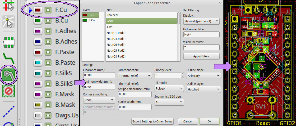
Filling an area with copper
Repeat this process for the back copper layer. Once both planes are drawn, I usually hide them; it’s distracting to have most of the board always filled with a gold color. There are three buttons on the left sidebar you can use for toggling the visibility of filled zones:
![]()
The top one makes filled zones fully visible, and the middle one hides them. Now, we can draw the actual connections.
To draw a copper trace, select either the front or rear copper layer, and press the x key to start drawing. Drawing a trace works just like drawing a wire in the schematic view, but their “corners” are at 45-degree angles instead of perpendicular. You can press the / key to change the next corner’s direction, and you can end a trace by right clicking and selecting the “End Track” option. Double-clicking also seems to work for ending a trace.
You can also press the v key to place a plated hole (called a “via”) and switch to the other side of the board. When you are not drawing a wire, the v key is a shortcut to switch between selecting the front and rear copper layers. Here are what a few example traces look like, in the power supply area, including a via to connect the tantalum capacitor on the rear of the board:
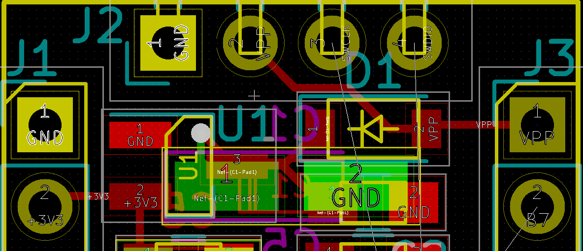
Some traces placed on the board
It is often a good idea to use wider traces than the default for power connections, but more advanced options like that are outside the scope of this basic tutorial. For low current at +3.3V, the default should be okay.
Now, you just have to connect the remaining lines. When you start drawing a trace on a pad, it will highlight the pad that you need to connect the trace to, so it’s pretty easy to just work your way through the board connecting the ‘guide’ lines. Here’s what I wound up with – I turned the copper fills back on to show the ground connections:
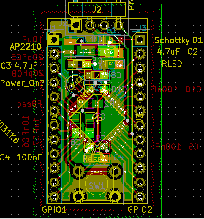
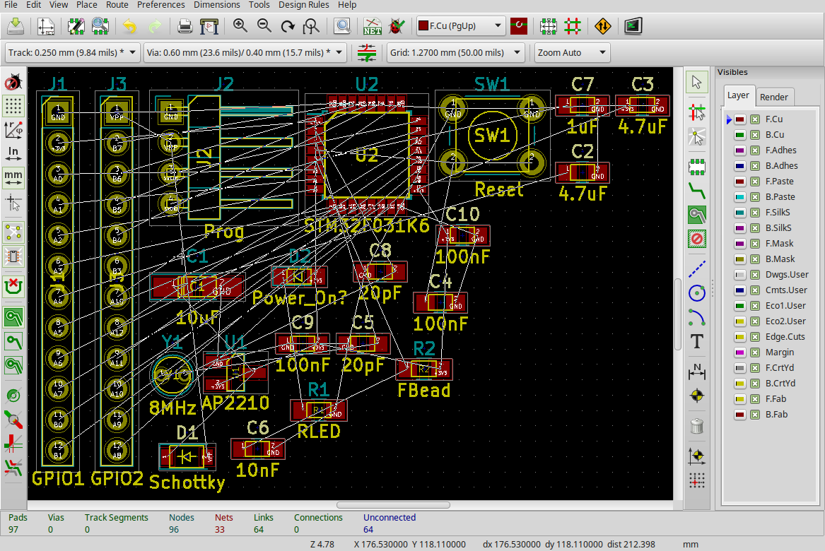
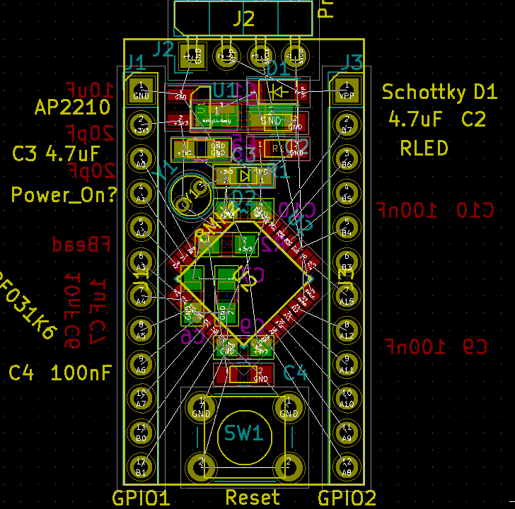
STM32 board, with all the pins connected
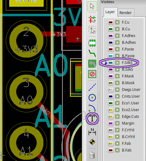
The only thing left to do is to label the pins on the silkscreen. You don’t want to have to check back to your schematic every time you want to use the board. You can use the ‘Text’ tool to add labels to a layer; make sure you have the front or rear silkscreen selected first. If the default text is too big, you can change the default size in the Dimensions -> Text and Drawing menu, or edit an individual label with the e key:
Adding labels to the pin headers: “3V3”, “A0”, “A1”, etc.
In addition to the pins, it’s also a good idea to label the + ends of polarized parts – like the tantalum capacitor and LED – with a label or marking.
Verifying the Design
Congratulations! Now you have your own complete design for an STM32F031K6 development board. KiCAD has some error-checking features which you should run before ordering anything, though. It’s easy to make small mistakes, and a short in the wrong place can completely break a design. When you run the design checks, it will automatically update your copper pours and tell you if any traces are too close together or intersecting. It can also check that none of the connections from the schematic are missing on the board.
So, open the design checking window by clicking on the button that looks like a bug with a check mark. To list any missing connections, click the ‘list unconnected’ button:
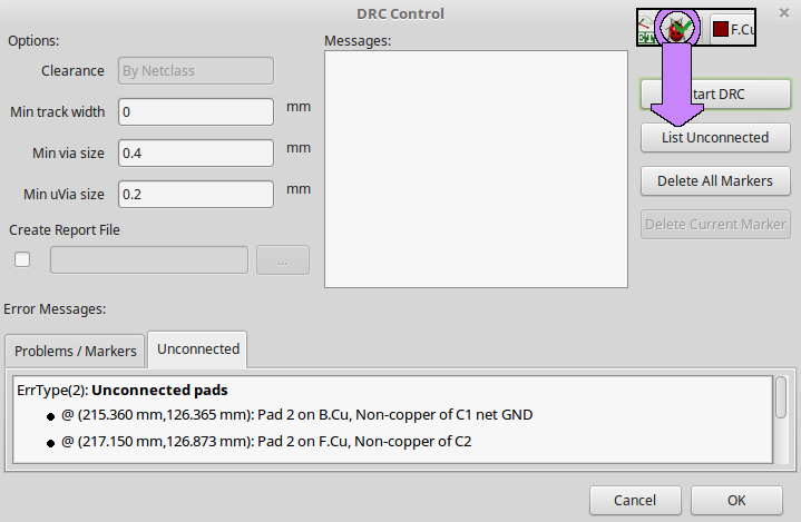
Using the “List Unconnected” check.
Whoops, there are a couple of unconnected pads. The most common connections that I miss are ones that are very close to each other on opposite sides of the board; the ‘guide’ lines can be almost invisible in those cases. You can double-click on one of the entries in the “Unconnected” panel near the bottom to center the view on it. Here’s the error that was called out in the above image, next to its fix:
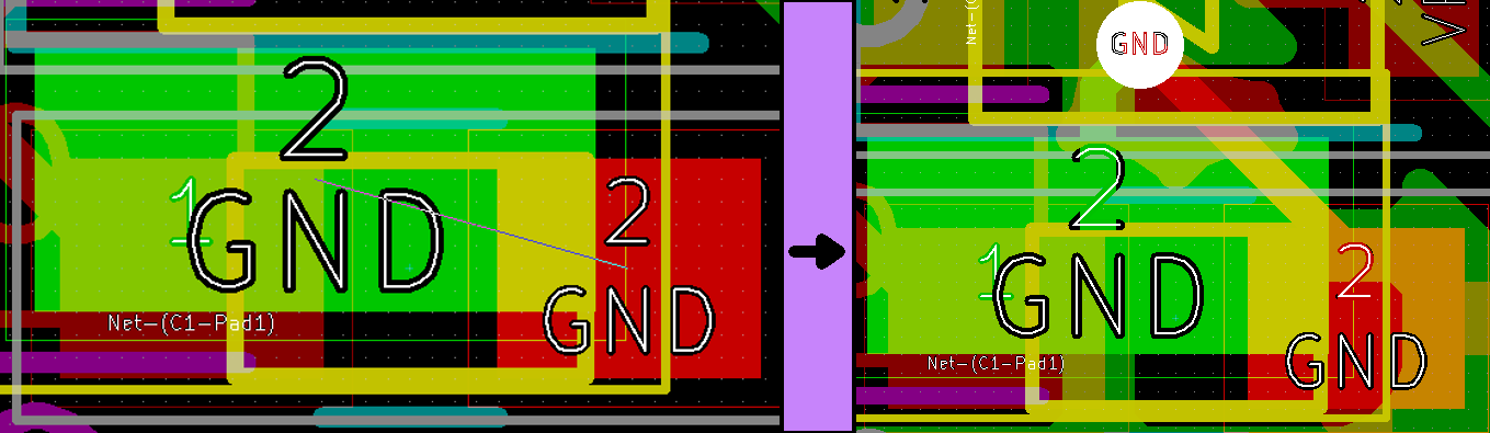
These nearby ground pins on opposite sides of the board weren’t connected, so I added a via
When there are no more missing connections, we can run the main design checks. click the “Start DRC” (Design Rules Check) button in the same view:
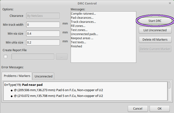
Running design rule checks
Huh, there are a bunch of “Pad near pad” errors. You can double-click on any one to center the view on it, and there are arrows drawn on the view near each error. Let’s take a look:
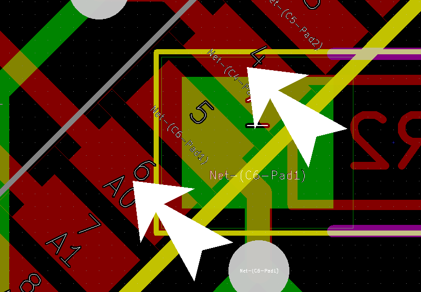
Arrows point to the reported errors.
Aha, the default QFP32 footprint’s pads are too close together for the default “Design Rules”. Fortunately, most PCB fabrication places have better capabilities than the defaults. I will use OSHPark’s settings, which are listed on their website. They can do 6 mil trace spacing, which equals 0.152 mm. To leave a margin of safety, I usually use 0.17 mm as a minimum clearance, but KiCAD’s default is 0.20 mm. To change that, use the Design Rules menu:
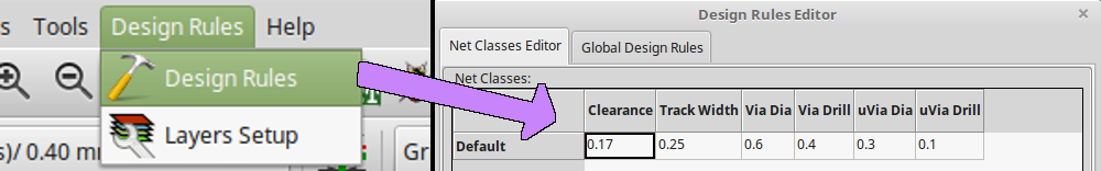
Changing the default clearance to 0.17mm
With that done, running the design checks doesn’t turn up any errors. Hit Ctrl+S, because now we’re finally ready to order the board!
Ordering Your Boards
There are a lot of options for ordering PCBs there days, and I don’t know about most of them. But OSHPark is very easy to use because they accept .kicad_pcb files instead of requiring you to fiddle around with exporting gerber files. They’re on the expensive end of things, but you can also use Seeed Studio’s “Fusion” service to get larger quantities made. A quick web search will probably bring up more options if you are interested, but I think that those are two reasonable places to start.
I ordered some of these boards from OSHPark; you can just sign up, upload the .kicad_pcb file in your project directory, and checkout like a normal online store. These boards cost a few cents more than $1.50 each (although that will depend on your board outline), and you can order them in multiples of 3. I got 6 for a little under $10, and they should arrive in a few weeks. I’ll write about assembling the boards then, and if they work I’ll make the OSHPark project public then.
Here’s what OSHPark renders:
OSHPark’s render of the board
Conclusions
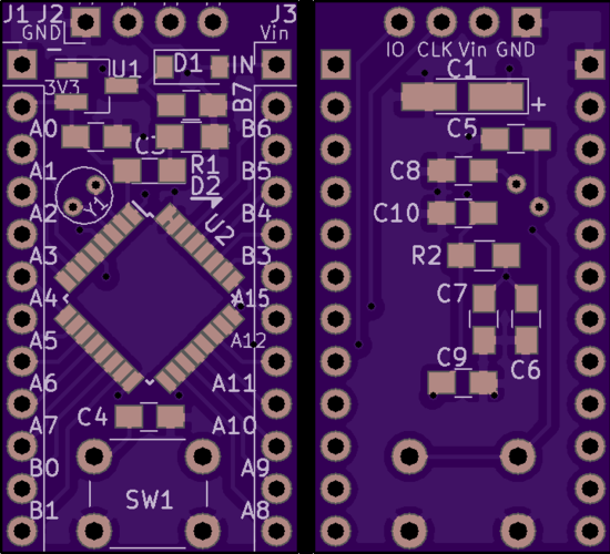
So I can’t say whether this particular design and layout will work until the boards arrive, but I have made several types of similar boards before and they seem okay – here’s how one recent version turned out:
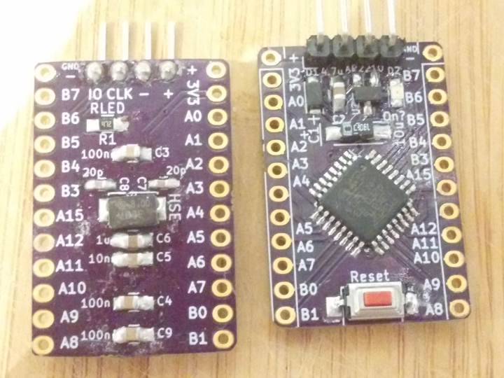
Some assembled STM32 breakout boards
You can use an inexpensive “ST-Link” USB debugger to connect to the Prog header and upload code to it. The ARM Cortex-M cores in the STM32 line of chips take a bit more initialization and configuring than simpler 8-bit microcontrollers, but they are powerful and they span a very wide range of power efficiency and performance.
Speaking of, this same design also works with other QFP32 STM32Fxxx chips, including the more powerful STM32F303K8. Double-check the pinouts listed in your chip’s datasheet, but I haven’t had any problems yet.
I’m sorry if there are any errors; this wound up being a pretty long tutorial, and I’d welcome corrections! And again, the example project is available on Github.
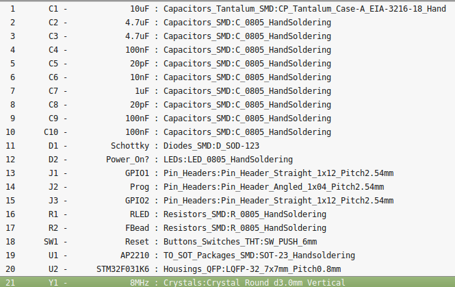
Bill of Materials
The only parts not included in this table are the ‘pin headers’. Those are much cheaper to buy from non-authorized distributors. For everything else, I’ve linked to a part on Digikey:
| Part Name | Footprint Size | Example Part | Quantity (per board) |
| 10uF Tantalum Capacitor | “A” / 1206 | Link | 1 |
| 4.7uF Ceramic Capacitor | 0805 | Link | 2 |
| 1uF Ceramic Capacitor | 0805 | Link | 1 |
| 100nF Ceramic Capacitor | 0805 | Link | 3 |
| 10nF Ceramic Capacitor | 0805 | Link | 1 |
| 20pF Ceramic Capacitor | 0805 | Link | 2 |
| Schottky Diode | SOD-123 | Link | 1 |
| LED | 0805 | Link | 1 |
| Resistor, 4.7KΩ | 0805 | Link | 1 |
| Ferrite Bead | 0805 | Link | 1 |
| 8MHz Crystal Oscillator | 3mm “Can” | Link | 1 |
| Reset Button | 6mm Push-Button | Link | 1 |
| AP2210-3.3 Voltage Regulator | SOT-23 | Link | 1 |
| STM32F031K6 Microcontroller | QFP-32 | Link | 1 |

karim
October 9, 2018 at 4:14 am
My brother suggested I might like this blog. He was entirely right. This post truly made my day. You can not imagine simply how much time I had spent for this info! Thanks!
Vivonomicon
October 16, 2018 at 10:40 am
Thanks, I’m glad you found it helpful – you might also look at ST’s application notes about hardware design, they are very helpful and pretty easy to read.
Like: ‘Getting started with STM32F10xx hardware development’
bot-10
October 1, 2019 at 8:58 pm
Better then gold, specifically your layout walkthrough
Vivonomicon
October 15, 2019 at 2:16 pm
Thank you for the kind words!
Ron Cromberge
October 15, 2018 at 11:53 am
Love your STM32 Articles!
Used your Kicad files and ordered 10 pcb’s by jclpcb.com And all the parts. Hope to see more STM32 posts.
Vivonomicon
October 16, 2018 at 10:24 am
Thanks, I am hoping to write some more when I have time – they’re fun little chips for learning about the Cortex-M architectures!
Ron Cromberge
November 13, 2018 at 7:03 am
Got my pcb’s from JclPcb. Only have to wait for the solder paste. 🙂 lot of patience when ordering from China. 🙂
Vivonomicon
November 17, 2018 at 7:38 pm
Good luck! I keep meaning to write the follow-up to this post, but the parts shouldn’t be too difficult to solder by hand or toaster.
jon
October 15, 2018 at 6:45 pm
Howdy very cool web site!! Man .. Beautiful .. Wonderful .. I will bookmark your web site and take the feeds additionally…I’m happy to search out numerous useful information right here in the post, we want work out extra techniques in this regard, thank you for sharing.
Vivonomicon
October 16, 2018 at 10:19 am
Thanks, I’m glad you like it! I am still learning as I write these, but KiCAD is turning out to be a lot of fun.
Badreddine
February 5, 2019 at 5:32 pm
I liked this tutorial. Very easy to follow…..
Andrius Kokianciks
April 14, 2019 at 6:03 am
Nice hard work. Thank You!
Mariwan
May 10, 2019 at 8:25 am
The picture you are showing for the board and the schematic/pcb drawn is not the same. Look at the switch. Why they are differ?
Thanks
Vivonomicon
May 13, 2019 at 9:03 am
I used to get confused by the 4-pin buttons a lot, too! A lot of switches have two or more pins connected to each side of the button, or sometimes they will have extra un-connected pins for extra stability when they are mounted to a board. So while the schematic only shows two pins on the switch, the footprint has four. That’s also why there is a trace connecting two of the button’s pins; it isn’t necessary because they are already connected inside of the switch, but I haven’t figured out how to stop KiCAD from thinking that those cases are “disconnected pin” errors.
Does that make sense, or did I accidentally mix up some screenshots somewhere? Sorry if I misunderstood your question.
Mariwan
May 27, 2019 at 10:42 pm
Thank you for your reply.
The picture of assembled boards are not representing the tutorial. They are for other designs. Look at the place of the LED, the switch ..etc all differ.
Any way, even I can KICAD, and most of the topic you mentioned here, I see your tutorial so interesting that I cannot leave it without reading it several times. I really enjoy it. Thanks 😉
Vivonomicon
May 30, 2019 at 8:23 am
You’re right, I hadn’t got the boards back when I wrote the post, so I used a picture of a similar design I had used in the past. I wanted to make a follow-up post about how to assemble the board, but I’m not exactly an expert on soldering and I don’t want to give bad advice.
But now that I do have a few of these boards, I should update that picture. Thanks for pointing that out.
Phobos
June 30, 2019 at 9:35 am
This post is awesome. Im really grateful. Please keep going!
Jithin
August 16, 2019 at 8:37 am
Hats off to your effort.. Thanks for all the information
Vivonomicon
August 22, 2019 at 10:38 am
Thank you, and good luck with your projects!