
OLED displays are excellent solutions for low-power, high-visibility UIs that don’t need to depict much detail and can be smaller than a square-inch or two. These days, they are cheap and available enough to be viable options for the hobbyist:
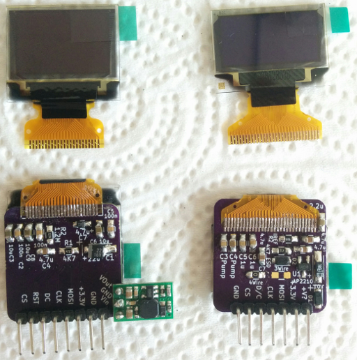
Top: The display panels as they arrive in the mail. Bottom: Boards with the circuits described in this post – the panels are glued to the other side.
These are two small display panels which you can find on Taobao, Alibaba, or eBay in small quantities for roughly $2-4 each. The one on the left is a 96×64-pixel SSD1331 16-bit color display. The one on the right is a 128×64-pixel SSD1306 monochrome display where each pixel is either ‘off’ or ‘on’ – typically ‘on’ is a white or blue color. Some of them have a row of 16px along the top set to yellow, but each pixel is still only one color.
In this post, we will walk through the circuitry (although not the code) required to control these displays using a microcontroller, including circuit schematics for laying out a ‘breakout board’ in your preferred EDA program – I used KiCAD, and I’ll also provide a link to those projects if you don’t want to design a new board.
Why? These boards are already cheap.
Okay, yes, you can buy these displays already soldered to a board with pins for easy I2C or SPI communications. And the SSD1306 boards cost less than $5 for the whole thing. But if we can make our own breakout board, we can also design these displays directly onto a broader device:
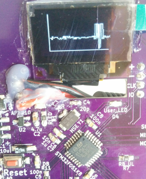
SSD1306 panel mounted on the first revision of a microcontroller board.
And as for the color displays, the prebuilt SSD1331 modules are actually fairly expensive, considering that the price difference between these panels is less than $2. They don’t have a built-in charge pump like the monochrome ones do, so we need to provide them with a separate power supply of something in the range of 12-18V. Most 3.3-5V microcontroller boards cannot supply that, so boost converters are generally added to the boards and that drives the cost up. I’ll ignore that problem for this tutorial by using a 12V Pololu step-up module in my design, but even with that extra expense you should only be looking at about $10-15 per board.
Plus your time of course, but learning how to use new parts is fun, right?
Typical 30-pin 128×64 SSD1306 Display
So let’s start with the 0.96″ 128×64-pixel monochrome SSD1306 display. One of its most common incarnations seems to be this 30-pin module with a 0.96″ display and polyimide ‘ribbon’ connector.
These display modules support I2C, SPI, and 8-pin parallel communication protocols. I haven’t tried the parallel protocols yet, so this post will only cover I2C and SPI designs.
To start, let’s look at the panel’s dimensions and layout. If it is facing us, then pins 1-30 will run from left to right, as indicated in the following image from a Taobao listing. The dimensions show that the entire connector is 22mm at its widest, with pins that are 0.4mm wide and spaced 0.7mm apart:
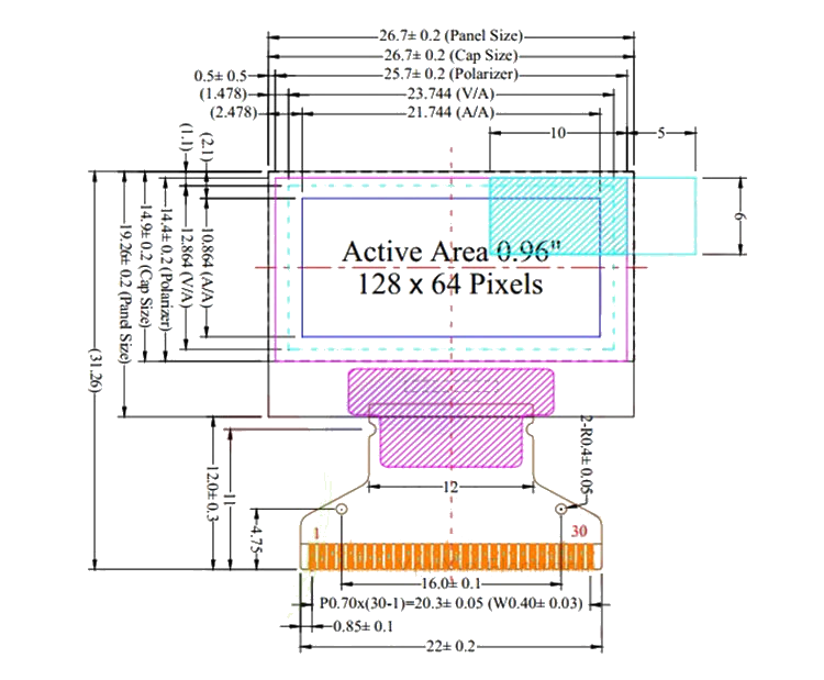
SSD1306 Panel Dimensions
I’ll link to a repository with ‘.kicad_mod’ files for connector footprints at the end of this post, but there should be enough information in that image to make your own footprint too. The pins’ functions will also hopefully be described in the listing that you buy from, but here are the descriptions that were provided with the ones I got, and the connections we will use in our circuit:
| Pin Number | Pin Symbol | Pin Function (mostly verbatim when relevant) | Our Circuit |
| 1 | N/C (GND) | The supporting pin can reduce the influences from stresses on the function pins. These pins must be connected to external ground as the ESD protection circuit. | GND |
| 2 | C2P | The charge-pump capacitors are required between these terminals. They must be floating when the converter is not used. | 1uF capacitor ‘+’ (first capacitor) |
| 3 | C2N | [ Same as ‘C2P’ ] | 1uF capacitor ‘-‘ (first capacitor) |
| 4 | C1P | [ Same as ‘C2P’ ] | 1uF capacitor ‘+’ (second capacitor) |
| 5 | C1N | [ Same as ‘C2P’ ] | 1uF capacitor ‘-‘ (second capacitor) |
| 6 | VBAT | This is the power supply pin for the internal buffer of the DC/DC voltage converter. It must be connected to external source when the converter is used. It should be connected to VDD when the converter is not used. | 3.3V+ |
| 7 | N/C | The N.C. pin between function pins are reserved for compatible and flexible design. | (Floating) (The extra space really is helpful when using 0805 parts) |
| 8 | VSS | This is a ground pin. It acts as a reference for the logic pins. It must be connected to external ground. | GND |
| 9 | VDD | This is a voltage supply pin. It must be connected to external source. | 3.3V+ |
| 10 | BS0 | These pins are MCU interface selection input. See the following table [not shown, see text below]: | GND for I2C or 4-wire SPI 3.3V+ for 3-wire SPI |
| 11 | BS1 | These pins are MCU interface selection input. See the following table [not shown, see text below]: | GND for 3-wire or 4-wire SPI 3.3V+ for I2C |
| 12 | BS2 | These pins are MCU interface selection input. See the following table [not shown, see text below]: | GND |
| 13 | CS | This pin is the chip select input. The chip is enabled for MCU communication only when CS is pulled low. | “Chip Select” (SPI, to microcontroller) GND (I2C) |
| 14 | RES | This pin is reset signal input. When the pin is low, initialization of the chip is executed. Keep this pin pull high during normal operation. |
“Reset” (to microcontroller, or just pull-up)
|
| 15 | D/C | This pin is Data/Command control pin. When the pin is pulled high, the input at D7-D0 is treated as display data. When the pin is pulled low, the data at SDIN will be transferred to the command register. In I2C mode, this pin acts as SA0 for device address selection. | “Data/Command” (SPI, to microcontroller) GND (I2C) |
| 16 | R/W | [ This pin is only used in 8-bit parallel modes and is not relevant for I2C or SPI. ] | GND |
| 17 | E/RD | [ This pin is only used in 8-bit parallel modes and is not relevant for I2C or SPI. ] | GND |
| 18 | D0 | Data pin 0. SCL in I2C mode, SCK in SPI modes. (Clock pin) | “SCL” / “CLK” (to microcontroller) |
| 19 | D1 | Data pin 1. SDA in I2C mode, MOSI in SPI modes. There is no MISO on these displays’ SPI modes. | “SDA” / “MOSI” (to microcontroller) |
| 20 | D2 | Data pin 2. SDA in I2C mode (tie D1/D2 together), or leave floating in SPI modes. | “SDA” (I2C, tie to D1) Floating (SPI) |
| 21 | D3 | Data pin 3. Only used in 8-bit parallel modes. | GND |
| 22 | D4 | Data pin 4. Only used in 8-bit parallel modes. | GND |
| 23 | D5 | Data pin 5. Only used in 8-bit parallel modes. | GND |
| 24 | D6 | Data pin 6. Only used in 8-bit parallel modes. | GND |
| 25 | D7 | Data pin 7. Only used in 8-bit parallel modes. | GND |
| 26 | IREF | This pin is segment current reference pin. A resistor should be connected between this pin and VSS. Set the current at 12.5uA maximum. |
Connect a 330K-1.2M resistor (typically 910K) between this pin and ground.
|
| 27 | VCOMH | This pin is the input pin for the voltage output high level for COM signals. A capacitor should be connected between this pin and VSS. |
Connect a ~4.7uF capacitor between this pin and ground. Do NOT connect this pin to 3.3V+
|
| 28 | VDisplay | This is the most positive voltage supply pin of the chip. A stabilization capacitor should be connected between this pin and VSS when the converter is used. It must be connected to external source when the converter is not used. |
Connect a ~2.2uF capacitor between this pin and ground. Do NOT connect this pin to 3.3V+
|
| 29 | VLSS | This is an analog ground pin. It should be connected to VSS externally. | GND |
| 30 | N/C (GND) | The supporting pin can reduce the influences from stresses on the function pins. These pins must be connected to external ground as the ESD protection circuit. | GND |
In addition to those connections, we will place a couple of 1uF decoupling capacitors across the positive voltage supplies at pins 6 and 9, and a simple Resistor/Capacitor/Diode filter on the reset pin with values of 4.7uF and 4.7KΩ. The diode might not be necessary, but I think that it improves the filter’s power efficiency a tiny bit?
Anyways, that’s a lot of information to convey in table and paragraph form. Here is a schematic for the SPI configuration:
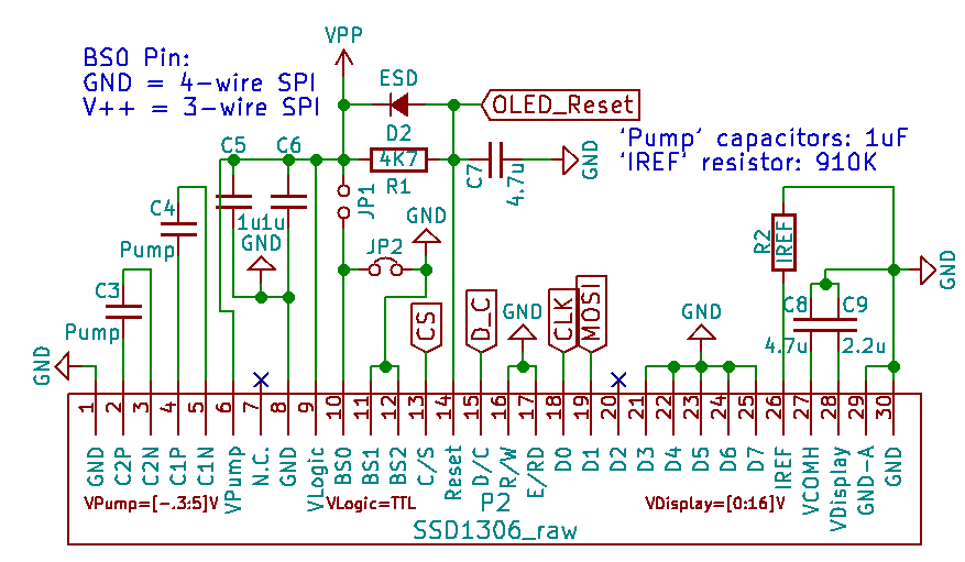
SSD1306 circuit
The circuit for I2C communication looks similar – just change the BS0/1/2 pins to Low/High/Low, tie the D1/D2 pins together, and pull the ‘CS’ pin to ground. The ‘D/C’ pin would determine the device’s I2C address, between 0x7A (high) and 0x78 (low).
You don’t need to connect the ‘OLED_Reset’ label if you don’t plan on doing software resets – I didn’t include a reset pin on the example SSD1306 board linked at the end of this post, and it still works fine.
When laying out this circuit, you’ll probably want to place all of the components on the same side of the board as the ribbon connector’s footprint. That will let you wrap the screen around to the other side of the board, and glue it to the flat surface. And be sure to double check the orientation of pins ‘1’ and ’30’ on your ribbon footprint – don’t get them flipped by 180 degrees! You can design your board to be roughly 1″ in each dimension – it might look something like this:
Renders of an example SSD1306 SPI board – the ground plane is omitted in the right image. Hopefully you can lay out a cleaner silkscreen…
The extra SOT-23 chip is just an AP2210 voltage regulator, to bring a 5-12V input down to 3.3V for the display. Once your boards arrive, you can assemble them normally. I don’t think the display panels would survive reflow soldering, but it is very easy to hand-solder the ribbon connectors with a bit of solder paste and a footprint that leaves solder resist between each pin.
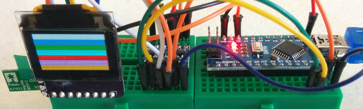
Once the board is soldered, we can quickly test that the assembled boards actually work with an ‘Arduino’ and Adafruit’s SSD1306 libraries – these displays seem to be designed for 3.3V and some of the maximum ratings are as low as 3.5V, so I would strongly advise using a level shifter if your board uses 5V logic:
Working SSD1306 display, driven by an ATMega328p Nano board through a level shifter.
That said, if you’re short on parts and just want to run a test, I did try using raw 5V logic from the Arduino, and it did seem to work. Doing that might damage the display, but who knows, it also might not.
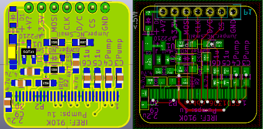
Typical 23-pin 96×64 SSD1331 Display
So that’s fun and all, but only having one pixel color available is awfully limiting. Enter the SSD1331 panel and its 16 bits of color per pixel. You get fewer pixels with its 96×64 resolution, but…colors! Here are the dimensions for a 23-pin panel which seems to be fairly common:
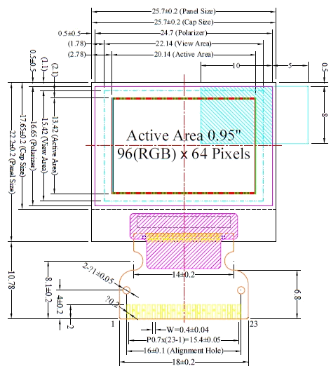
SSD1331 Panel Dimensions
Like the SSD1306 display, we have 0.4mm-wide pins spaced every 0.7mm, and the cable is 18mm at its widest. Again, a footprint file is available in the repository at the end of this post along with a copy of the KiCAD project for the rough-around-the-edges breakout board described below.
Here are the connector’s pin numbers, descriptions, and usage in our example SPI breakout board – again, with the panel facing us and the ribbon extending below it, the pins run left-to-right from 1-23 as shown in the image. Unlike the SSD1306 panels, this display does not support the I2C interface.
| Pin Number | Pin Symbol | Pin Function (mostly verbatim when relevant) | Our Circuit |
| 1 | N/C | The supporting pins can reduce the influences from stresses on the function pins. | Floating |
| 2 | VSS | This is a ground pin. It also acts as a reference for the logic pins, the OEL driving voltages, and the analog circuits. It must be connected to external ground. | GND |
| 3 | VDD | This is a voltage supply pin. It must be connected to external source. | 3.3V+ |
| 4 | VDDIO | It should be match with the MCU interface voltage level. VDDIO must always be equal or lower than VDD. | 3.3V+ |
| 5 | BS1 | These pins are MCU interface selection input. [0/0 for SPI] | GND |
| 6 | BS2 | These pins are MCU interface selection input. [0/0 for SPI] | GND |
| 7 | IREF | This pin is segment current reference pin. A resistor should be connected between this pin and VSS. Set the current at 10uA. |
Connect a 910K-1.2M resistor between this pin and ground.
|
| 8 | CS | This pin is the chip select input. The chip is enabled for MCU communications only when CS is pulled low. |
“CS” (to microcontroller)
|
| 9 | RST | This pin is reset signal input. When the pin is low, initialization of the chip is executed. |
“Reset” (to microcontroller, or just pull-up)
|
| 10 | D/C | This pin is Data/Command control pin. When the pin is pulled high, the input at D0-D7 is treated as display data. When the pin is pulled low, the input at D0-D7 will be transferred to the command register. |
“D/C” (to microcontroller)
|
| 11 | R/W (WR) | [ This pin is only used by 8-bit parallel communication; pull to ground for SPI. ] | GND |
| 12 | E (RD) | [ This pin is only used by 8-bit parallel communication; pull to ground for SPI. ] | GND |
| 13 | D0 | [ Data pin 0. “CLK” in SPI mode. ] | “CLK” (to microcontroller) |
| 14 | D1 | [ Data pin 1. “MOSI” in SPI mode. ] | “MOSI” (to microcontroller) |
| 15 | D2 | [ Data pin 2. Pull to ground in SPI mode. ] | GND |
| 16 | D3 | [ Data pin 3. Pull to ground in SPI mode. ] | GND |
| 17 | D4 | [ Data pin 4. Pull to ground in SPI mode. ] | GND |
| 18 | D5 | [ Data pin 5. Pull to ground in SPI mode. ] | GND |
| 19 | D6 | [ Data pin 6. Pull to ground in SPI mode. ] | GND |
| 20 | D7 | [ Data pin 7. Pull to ground in SPI mode. ] | GND |
| 21 | VCOMH | The COM signal deselected voltage level. A tantalum capacitor should be connected between this pin and VSS. |
Connect a 4.7uF tantalum capacitor between this pin and ground. Don’t connect this pin to a positive voltage supply.
|
| 22 | VCC | This is the most positive voltage supply of the chip. It should be supplied externally. [Display voltage] | 12V+ |
| 23 | N/C | The supporting pins can reduce the influences from stresses on the function pins. | Floating |
Applying that information, here is a circuit for one of these SSD1331 displays. The 3-pin connector is for the previously-mentioned 12V step-up board from Pololu, but you can use any converter that will take 3.3-5V and bump it up to 12-18V:
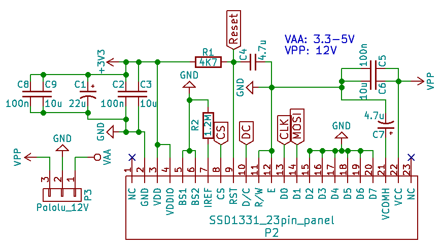
SSD1331 Circuit
The recommended decoupling capacitors here appeared to be a 10uF/100nF pair for each voltage input pin, a 4.7uF tantalum capacitor for the ‘VCOMH’ pin, and a large-ish tantalum capacitor (I went with 22uF) on the logic-level voltage supply. Some more decoupling on the step-up converter’s output might be a good idea, but this seems to work.
I also removed the reset filter’s diode on this board, and while I left the two outside ‘strain relief’ pins floating, maybe it would be better to pull them to ground like in the SSD1306 circuit.
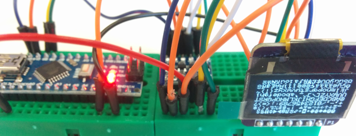
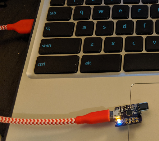
You can assemble the boards the same way as with the SSD1306 ones; mostly normally, but don’t put the display panel in a reflow oven. And again, the recommended logic level is 3.3V; the pins probably aren’t rated for 5V operation. This board does seem to work with an Arduino’s 5V logic for testing if that’s all you have in arm’s reach, but again, I’d recommend using 3.3V logic:
Working SSD1331 display, also driven by a Nano board through a level shifter.
Funny story though, this SSD1331 display does more than just work with 5V logic. It seems to work fine with the “+3.3V” supply completely disconnected and unpowered. The only power input was 12V on the VCC pin (#22) and the data pins were receiving 5V logic, but it still worked. I would not recommend doing that, but it’s interesting.
Conclusions
It looks like these displays are pretty robust, considering the conditions that I wound up testing them under and my supporting circuit design/layout, which I’m guessing is not great. They also don’t consume much power, and they are much more visible under bright lights than traditional LCD or TFT displays. And to top it all off, they’re very cheap – I got these panels for $2.00 per SSD1306 and $3.50 per SSD1331 (before international shipping.)
Still, a disclaimer: I thought that it might be worth sharing these circuits because I had trouble finding ones that worked, the displays look great, and the individual panels are affordable for hobbyists on a budget. But I couldn’t find much design documentation for these, and I don’t have much experience with designing circuit boards. Feedback or corrections are very welcome.
Also, while a big part of what makes these displays appealing is their low cost, let’s not forget that Adafruit wrote those easy-to-use Arduino libraries that I used earlier in the post to verify that the boards were working. If you want a “known-good” board to test against, or just need a working screen in a few days, they sell ready-to-use boards with these types of displays such as:
And I notice that their SSD1331 boards include onboard logic level shifters and a microSD card slot, so it’s not like you don’t get anything for the extra money.
Anyways, here is a Github repository with KiCAD projects for both of the boards shown in this post, and footprint/schematic library files for the ribbon connectors described above. These aren’t production-ready designs or anything, but they appear to work and can hopefully get you get started:
I’d like to follow up with a post about driving these OLED displays using STM32 boards, but I am behind on posts about those chips already; I still have to finish the one about writing basic ‘boot’ code and getting them to run a familiar-looking ‘main’ C function. I hope this was helpful or interesting!

Edwin
December 4, 2018 at 4:57 pm
Did you get around writing up an stm32 version? If not I have managed to port an SSD1306 library I found to stm32 which I use to drive these little displays. It just a matter of providing the hardware functions to transmit whatever the library outputs. I am now trying to integrate them onto my own pcb so I cam across your post , i just have to figure out a way to convert those kicad files to Altium or switch my project to kicad. either way thanks for the info.
Vivonomicon
December 5, 2018 at 7:57 pm
Well I did write a post about using the SSD1331 OLED with a software SPI interface, but unfortunately the commands are going to be a bit different for the SSD1306 since it is monochrome. If you only need a sequence of commands to initialize and draw to the screen, I did write some C++ classes for the STM32 I2C peripheral and using that with the SSD1306:
https://github.com/WRansohoff/STM32_CPP_Inheritance
That said, you might also want to look into a more polished library such as libopencm3 – but be aware that it is GPLv3 if you do decide to use it:
https://github.com/libopencm3/libopencm3
There are also a few good FOSS embedded GUI libraries, such as uGUI:
https://embeddedlightning.com/ugui/
Good luck!