Microcontrollers are just like any other kind of semiconductor product. As manufacturers learn from customer feedback and fabrication processes continue to advance, the products get better. One of the most visible metrics for gauging a chip’s general performance – and the basis of Moore’s Law – is how large each transistor is. Usually this is measured in nanometers, and as we enter 2019 the newest chips being made by companies like Samsung and Intel are optimistically billed as 7nm.
The venerable and popular STM32F1 series is more than a decade old now, and it is produced using a 130nm process. But ST’s newer lines of chips like the STM32L4 use a smaller 90nm process. Smaller transistors usually mean that chips can run at lower voltages, be more power-efficient, and run at faster clock speeds. So when ST moved to this smaller process, they introduced two types of new chips: faster ‘mainline’ chips like the F4 and F7 lines which run at about 100-250MHz, and more efficient ‘low-power’ chips like the L0 and L4 lines which have a variety of ‘sleep’ modes and can comfortably run off of 1.8V. They also have an H7 line which uses an even smaller 40nm process and can run at 400MHz.
Now as 2018 fades into history, it looks like ST has decided that it’s time for a fresh line of ‘value-line’ chips, and we can order a shiny new STM32G0 from retailers like Digikey. At the time of writing there aren’t too many options, but it looks like they’re hoping to branch out and there are even some 8-pin variants on the table. I could be misreading things, but these look like a mix between the F0 and L0 lines, with lower power consumption than F0 chips and better performance than the L0 chips. The STM32G071GB that I made a test board with has 128KB of Flash, 36KB of RAM, and a nice set of communication peripherals.
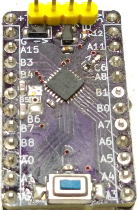
Simple STM32G0 breakout board
So what’s the catch? Well, this is still a fairly new chip, so “Just Google It” may not be an effective problem-solving tool. And it looks like ST made a few changes in this new iteration of chips to provide more GPIO pins in smaller packages, so the hardware design will look similar but slightly different from previous STM32 lines. Finally, with a new chip comes new challenges in getting an open-source programming and debugging toolchain working. So with all of that said, let’s learn how to migrate!
Hardware Design
I chose the STM32G071GB for the simple reason that it was the only G0 chip that I could find in stock anywhere; it looks like stocks are starting to replenish, but I guess that new parts sell out quickly, and I didn’t notice that these chips existed until after the winter holidays. ST does sell an $11 Nucleo board with a 64-pin version of the chip if you’re reading this from a better-stocked future, but I had to take what I could get and refer to their ‘Getting Started with Hardware Development‘ guide, which is available along with several other useful chip-specific documents on ST’s website.
There are a few differences between the basic F0 / L0 design that I wrote about previously and these G0 chips, but the power supply looks mostly the same. Your external voltage regulator should have a >= 4.7μF decoupling capacitor, and another 100nF decoupling capacitor is required near the voltage supply pins. The small 28-pin QFN package has no VREF+ pin for providing a separate analog supply voltage, so while the analog peripherals will be stuck using the noisy digital supply in this design, we can also use fewer filtering passives.
Next up is the reset pin, which can actually be configured as a normal GPIO pin on an STM32G0 chip. But its default behavior is still to act as a reset pin and it is nice to include a reset button on a simple breakout board, so I connected it to the usual push-button with a 10nF decoupling capacitor.
There are also no differences in the external oscillator wiring; the 28-pin package does not have space for an HSE high-speed oscillator, but it does have room for an LSE low-speed oscillator so I included a small 32.768KHz crystal with 5pF capacitors decoupling each side.
And finally, there is no BOOT0 pin! Previous STM32 lines have always had an external pin to select where in memory the chip should boot from, and this was often a source of confusion for new designers. It looks like the default configuration is now to ignore the external boot signal and start from the main flash memory (see section 3.4.1 in the reference manual), and the BOOT0 pin is now shared with the SWCLK debugging pin if you really need to use it. We don’t need it for a basic breakout board, so we don’t need to worry about boot configuration with these new chips. Hooray!
The debugger wiring also looks the same, with a data and clock line that can connect to an external device. So once I added pin connectors for the GPIO pins and a programming header, here is the circuit I ended up with:
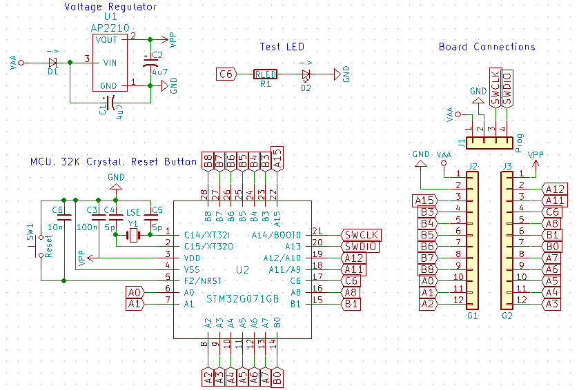
STM32G071GB minimal schematic
The 3-pin linear voltage regulator is a 3.3V AP2210, but it looks like these chips should work within a range of 1.8V – 3.6V.
Toolchain Support
We shouldn’t need to make many changes to our build process, because the G0 line uses the same ARM Cortex-M0+ core as the L0 line. The same arm-none-eabi-gcc commands will work, and these chips aren’t so new that ST doesn’t provide software support; the STM32Cube G0 package contains device header files for the chips.
But I use an open-source stlink tool written by Texane to upload code to the chip once it is compiled, and I’m not sure if it supports this new chip yet. I can find out by running st-util to try connecting to the chip:
INFO common.c: Loading device parameters....
WARN common.c: unknown chip id! 0x20006460
It looks like the tool doesn’t recognize the chip’s identifier. It’s sort of difficult to search for information about the IDs which identify different lines of STM32 chips, and they can be confusing because sometimes chips with different part numbers can share the same ID. I couldn’t find a central listing of all STM32 IDs, but they are usually listed in each individual chip’s reference manual. Look at section 37.10.1, ‘DBG device ID code register’; it lists 0x460 for G071xx and G081xx devices.
So we’ll need to add this chip ID to the program’s list of valid ones, and give it a bit more information about the chip which we can also find in the reference manual. And it looks like the most important Flash registers in the STM32G0 are also offset by one word compared to most of its STM32Fx and Lx cousins, so we’ll also need to write a few small methods for the core Flash operations of ‘erase page’ and ‘write words’. When I wrote this, the current version of the stlink tool was 7651d21 – you can check that out if you want to follow along.
Adding a new chip ID
Usually when I run into an error, I try to find where it came from by searching for the error message:
> grep -R "unknown chip id!" *
src/common.c:        WLOG("unknown chip id! %#x\n", chip_id);
Looking in the src/common.c file, the error is logged if a call to stlink_chipid_get_params fails. That method is in the src/chipid.c file, and directly above it is a large struct definition called stlink_chipid_params_devices. It looks like that struct contains all of the recognized chips, so let’s add one for STM32G071xx/G081xx chips. Here is an example definition for an L4 chip:
{
    // STM32L4x6
    // From RM0351.
    .chip_id = STLINK_CHIPID_STM32_L4,
    .description = "L4 device",
    .flash_type = STLINK_FLASH_TYPE_L4,
    .flash_size_reg = 0x1FFF75e0,    // "Flash size data register" (sec 45.2, page 1671)
    .flash_pagesize = 0x800,         // 2K (sec 3.2, page 78; also appears in sec 3.3.1 and tables 4-6 on pages 79-81)
    // SRAM1 is "up to" 96k in the standard Cortex-M memory map;
    // SRAM2 is 32k mapped at at 0x10000000 (sec 2.3, page 73 for
    // sizes; table 2, page 74 for SRAM2 location)
    .sram_size = 0x18000,
    .bootrom_base = 0x1fff0000,      // Tables 4-6, pages 80-81 (Bank 1 system memory)
    .bootrom_size = 0x7000           // 28k (per bank), same source as base
},
We can find similar information in the G071/081 reference manual, and add another entry:
{
    // STM32G071/081 (from RM0444)
    .chip_id = STLINK_CHIPID_STM32_G0X1,
    .description = "G071/G081 device",
    .flash_type = STLINK_FLASH_TYPE_G0,
    .flash_size_reg = 0x1FFF75E0,    // Section 38.2
    .flash_pagesize = 0x800,         // 2K (sec 3.2)
    .sram_size = 0x9000,             // 36K (sec 2.3)
    .bootrom_base = 0x1fff0000,
    .bootrom_size = 0x7800           // 30K (table 2)
},
We’ll also need to add the STLINK_FLASH_TYPE_G0 constant to the stlink_flash_type enum which is located in include/stlink.h, and add STLINK_CHIPID_STM32_G0X1 = 0x460 to the stlink_stm32_chipids enum in include/stlink/chipid.h. Let’s try building the project and seeing what happens now. Fortunately, stlink is easy to build (see the project’s compiling guide for more information about dependencies etc):
cmake .
make
You can also install the tool system-wide with sudo make install, but it can be a little risky to do that when you’re not sure if the new version will work properly. The st-util program is built under src/gdbserver, and if you run ./st-util it should connect to the chip:
INFO usb.c: -- exit_dfu_mode
INFO common.c: Loading device parameters....
INFO common.c: Device connected is: G071/G081 device, id 0x20006460
INFO common.c: SRAM size: 0x9000 bytes (36 KiB), Flash: 0x20000 bytes (128 KiB) in pages of 2048 bytes
INFO gdb-server.c: Chip ID is 00000460, Core ID is  0bc11477.
INFO gdb-server.c: Listening at *:4242...
But if you try to upload a test program, no luck:
> ./st-flash write main.bin 0x08000000
INFO usb.c: -- exit_dfu_mode
INFO common.c: Loading device parameters....
INFO common.c: Device connected is: G071/G081 device, id 0x20006460
INFO common.c: SRAM size: 0x9000 bytes (36 KiB), Flash: 0x20000 bytes (128 KiB) in pages of 2048 bytes
INFO common.c: Attempting to write 456 (0x1c8) bytes to stm32 address: 134217728 (0x8000000)
WARN common.c: unknown coreid bc11477, page erase failed
ERROR common.c: Failed to erase_flash_page(0x8000000) == -1
stlink_fwrite_flash() == -1
The relevant error message is, “unknown coreid bc11477, page erase failed”. The actual flash commands sometimes differ between different lines of chips, and those commands aren’t written for STLINK_FLASH_TYPE_G0 yet because we only just added it. Like I mentioned above, it looks like the core Flash registers are in a slightly different location on G0 chips so we can’t re-use the logic for a similar line. But the peripheral still works the same, so we can get a minimal working version using the same sequence of commands.
Updating Flash Commands
If you search for the ‘unknown coreid’ error message, you’ll see that this logic is located in the src/common.c file which defines three common operations that we will need to implement: stlink_erase_flash_page, stlink_write_flash, and stlink_erase_flash_mass. And it’s lazy, but that can be further reduced to two operations if we mimic the STM32L0 ‘mass erase’ function to simply call ‘erase page’ in a loop.
So you can find this process in section 3 (“FLASH”) of the reference manual, but follow the same basic steps to erase and write to flash memory. To erase a page:
- Unlock the Flash.
- Set the ‘page erase’ PER bit in the CR ‘control register’.
- Set which page to erase in the PNB ‘page number bits’ in CR.
- Set the ‘start’ STRT bit in CR.
- Wait for the ‘busy’ BSY bit in SR.
- Un-set the PER bit.
- Lock the flash.
And to write a sequence of bytes:
- Unlock the Flash.
- Set the ‘enable programming’ PG bit in CR.
- Write the next byte of data to its location in Flash.
- Wait for the ‘busy’ BSY bit in SR.
- Go to step 3 if there is more data to send.
- Send one ‘dummy word’ if an odd number of bytes were sent (Flash is programmed 2 words at a time).
- Un-set the PG bit.
- Lock the flash.
I won’t copy all of the code here, but you can find it in this Github fork of the project. Once those changes have been made, you should be able to make the project again. And this time, the st-flash command should succeed:
> st-flash write main.bin 0x08000000
INFO usb.c: -- exit_dfu_mode
INFO common.c: Loading device parameters....
INFO common.c: Device connected is: G071/G081 device, id 0x20006460
INFO common.c: SRAM size: 0x9000 bytes (36 KiB), Flash: 0x20000 bytes (128 KiB) in pages of 2048 bytes
INFO common.c: Attempting to write 456 (0x1c8) bytes to stm32 address: 134217728 (0x8000000)
Flash page at addr: 0x08000000 erased
INFO common.c: Finished erasing 1 pages of 2048 (0x800) bytes
INFO common.c: Starting verification of write complete
INFO common.c: Flash written and verified! jolly good!
I’m not sure if any verification is actually performed – I didn’t add any and it might just gloss over that, but it might also just read the flash addresses using generic commands since I think the locks only apply to writing. Anyways, the example program I used is just a test which blinks an LED on pin C6, which you can find on Github here. And what do you know, it looks like it works!
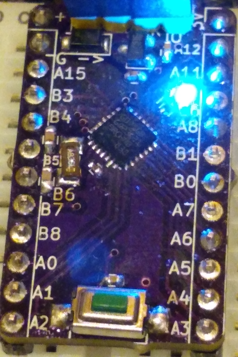
STM32G0 with a blinking LED
Conclusions
It’s nice to be able to try new chips like this if you want to play with them, but keep in mind that this probably won’t be the fastest way to test an application on new hardware. I was going to use one of ST’s Nucleo boards, which would have been a lot faster if they hadn’t been sold out at the time. And ST distributes a free tool for programming their chips, but it’s not Free-with-a-capital-F so it probably wouldn’t work on say, a Raspberry Pi. Still, it’s fun and who doesn’t like playing with new toys?
Finally, a quick disclaimer that I have not extensively tested this code and there could be issues with it. Just because it worked with a single small test program doesn’t mean that it will work with all of the stlink project’s usual features. Suggestions are always welcome – good luck!