
I’ve written a few basic tutorials about bare-metal STM32 development in the past, and even though I’m still learning as I write them, I think that there’s enough groundwork to start covering some ‘real world’ scenarios now. I’d like to start with a very important technique for designing efficient applications: the Direct Memory Access (DMA) peripheral. DMA is important because it lets you move data from one area of memory to another without using CPU time. After you start a DMA transfer, your program will continue to run normally while the data is moved around ‘in the background’.
That’s the basic idea, but the devil is always in the details. So in this post, we’re going to review how the three main types of STM32 DMA peripherals work. Different STM32 chips can have similar peripherals which behave slightly differently, and usually more expensive / newer chips have more fully-featured peripherals. I think that this is how the peripherals are grouped, but I didn’t test every type of STM32 chip and corrections are always appreciated:
- ‘Type 1’ Simple DMA:
F0,L0,F1,L1,F3,L4 - ‘Type 2’ Double-buffered DMA:
F2,F4,F7 - ‘Type 3’ DMA + DMA multiplexer:
G0,G4,L4+
Once we’ve reviewed the basics of how DMA works, I’ll go over how to use it in a few example applications to show how it works with different peripherals and devices. The required hardware for each example will be discussed later, but I’ll present code to:
- Generate an audio tone by sending a sine wave to the DAC peripheral at a specific frequency.
- Map an array of colors to a strip of
WS2812orSK6812‘NeoPixel’ LEDs. - Map a small region of on-chip RAM to a monochrome
SSD1306OLED display. - Map a a region of RAM to an
ILI9163CorILI9341TFT display.
The key to these examples is that the communication with an external device will happen ‘in the background’ while your microcontroller’s CPU is doing other things. Most of the examples won’t even use interrupts; the data transmission is automatic once you start it. But be aware that DMA is not magic. Every DMA ‘channel’ or ‘stream’ shares a single data bus which is also used by the CPU for memory transfers, so there is a limit to how much data you can actually send at once. In practice this probably won’t be a problem unless you have multiple high-priority / high-speed DMA transfers with tight timing requirements, but it’s something to be aware of.
So let’s get started!
Part 1: Play a Musical Note on an STM32F3
To start with, let’s go over the most common type of STM32 DMA peripheral and use it to send some simple audio data to the chip’s DAC peripheral. I’ll be using an STM32F303 core for these examples; something like a ‘Nucleo-32‘ board or an ‘F3 Discovery Kit‘ should work.
Generating a musical note is pretty simple, we just need to send a sine wave to the DAC peripheral at the frequency of the tone that we want. To do that, we’ll have a buffer which holds equally-spaced ‘Y-axis’ values from a single [-π,π) cycle of sin(x), and we’ll send that buffer to the DAC peripheral in a loop. The frequency at which new data is sent to the DAC can be controlled using a timer peripheral, and we can verify that a 440Hz frequency produces an A4 note using a tuner. The more samples we use, the higher-resolution the sine wave will be and the better it will sound.
You’ll need an audio amplifier board and a small speaker to follow along with this example, and a tuner to test that it is accurate. I’ll use Adafruit’s MAX98306 breakout board with a small 8-Ohm speaker, but any amp should work.
‘Type 1’ DMA: F0/F1/F3/L0/L1/L4
Before writing any code, let’s review how the simplest type of STM32 DMA peripheral works in theory. A lot of this might be review if you’re already familiar with DMA and/or STM32 peripherals, so…sorry if it’s boring.
How Peripherals are Mapped to DMA Channels
‘Type 1’ STM32 DMA peripherals map each peripheral request signal to one of the several available DMA channels, but they don’t let you choose which peripherals map to which channels. You can find which peripherals are assigned to which channels in your chip’s reference manual; for the STM32F303 which will be used in the following example, check Table 78, “Summary of DMA requests for each channel” in Chapter 13 (DMA).
Since there are more peripherals than DMA channels, this style of mapping means you have to hope that all of the peripherals you want to use with DMA are mapped to different channels. ‘Type 3’ DMA peripherals offer more flexibility, but we’ll talk about that later. For now, just know that you can only use one peripheral with each DMA channel at any given time.
For example, our first demo will generate an audio waveform using the DAC peripheral. If you look at the STM32F303 reference manual’s DMA request mapping table, you’ll see that the DAC channel mappings have an extra footnote:
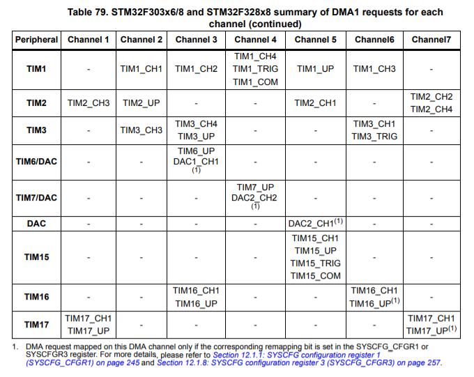
Notice the footnote attached to the ‘TIM6/DAC’, ‘TIM7/DAC’, and ‘DAC’ peripheral requests. And I’m not 100% sure, but I think ‘DAC2_CH2’ is a typo which should read ‘DAC1_CH2’.
Okay, it looks like we need to set a bit in one of the system configuration registers to enable the DAC’s DMA1 channel. There’s more information in the relevant register settings (under section 12.1, ‘SYSCFG Registers’):
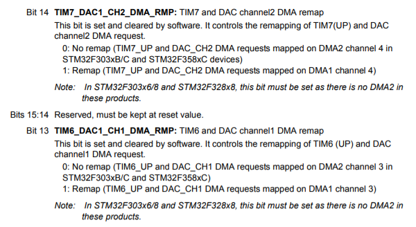
More information about DAC / DMA mapping. I’m not sure why it says that bits 14-15 are reserved – that might be a typo, because they seem to be used normally.
If you’re using a ‘Discovery Kit’ board, your STM32F303VC chip has two groups of DMA channels, and you can choose which one the DAC peripherals map to. If you’re using the ‘Nucleo-32’ board, your STM32F303K8 chip only has one group of DMA channels, and these bits need to be set if we want to use DMA with the DAC peripheral. So I’m going to set these bits and use DAC channel 1 with DMA1 channel 3.
Also, you might have noticed that the last two screenshots both had mildly confusing typos. Reference manuals are sometimes more what you’d call…guidelines, so try things out and use your own judgement if something looks wrong. And don’t judge the editors until you’ve tried proofreading one 🙂
Configuring DMA for Repeated Memory-to-Peripheral Transfers
Setting up a DMA transfer is not too complicated, but there are a handful of settings that you need to pay attention to. Ignoring interrupts and error events, you only need to worry about four registers for each DMA channel. One for configuration, one for holding the number of bytes to transfer, one for holding the ‘source’ address, and one for holding the ‘destination’ address.
When you want to send data from a region of memory to a peripheral, you usually put the starting memory address in the ‘source’ register (DMA_CMARx) and the peripheral’s register address in the ‘destination’ register (DMA_CPARx). The size of the memory region goes in the ‘number of bytes’ register (DMA_CNDTRx).
The ‘configuration’ (DMA_CCRx) register also needs to be set correctly. The MINC and PINC bits tell the peripheral whether it should increment the memory and peripheral addresses after each transfer, respectively. When we send data from memory to a peripheral, we usually want to set MINC and clear PINC so that the entire area of memory is sent to the same peripheral register.
There is also a CIRC bit, for ‘circular mode’. When it is set, the DMA peripheral will reload the original contents of its ‘source address’, ‘destination address’, and ‘number of bytes’ registers before starting a new transfer. Since we want to send a continuous stream of sine waves through the DAC peripheral, we should set the CIRC bit.
Finally, the MEM2MEM bit sets a special ‘memory-to-memory’ mode which ignores the usual DMA request triggers to transfer data as quickly as possible. It is useful for copying one area of internal memory to another, but it should not be set when peripherals are involved.
Those are the most important settings; the others are described in the example code’s comments and should be fairly self-explanatory.
Configuring the DAC Peripheral and Triggering DMA Transfers using a Timer
Each DAC channel on the STM32F3 series is only wired to one pin; in our case DAC1 channel 1 is connected to pin A4. Configuring the GPIO pin as a DAC output works the same as configuring it as an ADC input; just set the pin to Analog mode.
The STM32 DAC peripherals have some handy ‘trigger’ settings which let you synchronize the timing of DMA requests to signals like timers. The TSEL bits in the DAC_CR register configure the trigger source, and the TEN bit enables the trigger. There’s also a DMAEN bit which enables DMA requests from the DAC peripheral, and the usual EN bit to enable the peripheral. There are two sets of those bits, one for each DAC channel.
There are also a bunch of different data registers to use as a DMA ‘destination’, because the DACs are 12-bit and that doesn’t fit cleanly into 8 or 16-bit registers. I’ll use the right-aligned DAC_DHR12R1 register so that the values are between 0 and 4095.
Finally, you need to configure the timer specified in the TSEL bits. A lower prescaler is usually better when you want precision, because it makes the minimum time period smaller. These timers are only 16-bit, which means that they can only count up to 0xFFFF = 65,535, but that won’t be a problem in this example. The ‘autoreload’ ARR register tells the timer how many ticks to wait before restarting (and sending an ‘update’ signal), so we’ll set it to clock_speed / (tone_frequency * sine_samples). For a 440Hz 32-sample wave, that becomes 8,000,000/(440*32) = 568.
Putting it All Together
So let’s put that into code. This assumes the same sort of basic GCC/Make project setup as my past bare-metal STM32 tutorials, but it should probably work with any C project that includes the device header files distributed by ST.
// Standard library includes.
#include <stdint.h>
#include <stdlib.h>
// Vendor-provided device header file.
#include "stm32f3xx.h"

// 32-sample sine wave.
// (Use this macro to adjust aplitude/volume.)
#define _AMP(x) ( x / 2 )
const size_t SINE_SAMPLES = 32;
const uint16_t SINE_WAVE[] = {
  _AMP(2048), _AMP(2447), _AMP(2831), _AMP(3185),
  _AMP(3495), _AMP(3750), _AMP(3939), _AMP(4056),
  _AMP(4095), _AMP(4056), _AMP(3939), _AMP(3750),
  _AMP(3495), _AMP(3185), _AMP(2831), _AMP(2447),
  _AMP(2048), _AMP(1649), _AMP(1265), _AMP(911),
  _AMP(601),  _AMP(346),  _AMP(157),  _AMP(40),
  _AMP(0),    _AMP(40),   _AMP(157),  _AMP(346),
  _AMP(601),  _AMP(911),  _AMP(1265), _AMP(1649)
};

// Global variable to hold the core clock speed in Hertz.
uint32_t SystemCoreClock = 8000000;

// Simple imprecise delay method.
void __attribute__( ( optimize( "O0" ) ) )
delay_cycles( uint32_t cyc ) {
  for ( uint32_t d_i = 0; d_i < cyc; ++d_i ) { asm( "NOP" ); }
}

/**
 * Main program.
 */
int main(void) {
  // Enable peripherals: GPIOA, DMA, DAC, TIM6, SYSCFG.
  RCC->AHBENR   |= ( RCC_AHBENR_GPIOAEN |
                     RCC_AHBENR_DMA1EN );
  RCC->APB1ENR  |= ( RCC_APB1ENR_DAC1EN |
                     RCC_APB1ENR_TIM6EN );
  RCC->APB2ENR  |= RCC_APB2ENR_SYSCFGEN;

  // Pin A4: analog mode. (PA4 = DAC1, Channel 1)
  GPIOA->MODER    &= ~( 0x3 << ( 4 * 2 ) );
  GPIOA->MODER    |=  ( 0x3 << ( 4 * 2 ) );

  // Set the 'TIM6/DAC1 remap' bit in SYSCFG_CFGR1,
  // so that DAC1_Ch1 maps to DMA1_Ch3 instead of DMA2_Ch3.
  // (Not all STM32F303 chips have a DMA2 peripheral)
  SYSCFG->CFGR1 |=  ( SYSCFG_CFGR1_TIM6DAC1Ch1_DMA_RMP );

  // DMA configuration (DMA1, channel 3).
  // CCR register:
  // - Memory-to-peripheral
  // - Circular mode enabled.
  // - Increment memory ptr, don't increment periph ptr.
  // - 16-bit data size for both source and destination.
  // - High priority (2/3).
  DMA1_Channel3->CCR &= ~( DMA_CCR_MEM2MEM |
                          DMA_CCR_PL |
                          DMA_CCR_MSIZE |
                          DMA_CCR_PSIZE |
                          DMA_CCR_PINC |
                          DMA_CCR_EN );
  DMA1_Channel3->CCR |=  ( ( 0x2 << DMA_CCR_PL_Pos ) |
                           ( 0x1 << DMA_CCR_MSIZE_Pos ) |
                           ( 0x1 << DMA_CCR_PSIZE_Pos ) |
                           DMA_CCR_MINC |
                           DMA_CCR_CIRC |
                           DMA_CCR_DIR );
  // Set DMA source and destination addresses.
  // Source: Address of the sine wave buffer in memory.
  DMA1_Channel3->CMAR  = ( uint32_t )&SINE_WAVE;
  // Dest.: DAC1 Ch1 '12-bit right-aligned data' register.
  DMA1_Channel3->CPAR  = ( uint32_t )&( DAC1->DHR12R1 );
  // Set DMA data transfer length (# of sine wave samples).
  DMA1_Channel3->CNDTR = ( uint16_t )SINE_SAMPLES;
  // Enable DMA1 Channel 1.
  // Note: the transfer won't actually start here, because
  // the DAC peripheral is not sending DMA requests yet.
  DMA1_Channel3->CCR |= ( DMA_CCR_EN );

  // TIM6 configuration. This timer will set the frequency
  // at which the DAC peripheral requests DMA transfers.
  // Set prescaler and autoreload for a 440Hz sine wave.
  TIM6->PSC  =  ( 0x0000 );
  TIM6->ARR  =  ( SystemCoreClock / ( 440 * SINE_SAMPLES ) );
  // Enable trigger output on timer update events.
  TIM6->CR2 &= ~( TIM_CR2_MMS );
  TIM6->CR2 |=  ( 0x2 << TIM_CR2_MMS_Pos );
  // Start the timer.
  TIM6->CR1 |=  ( TIM_CR1_CEN );

  // DAC configuration.
  // Set trigger sources to TIM6 TRGO (TRiGger Output).
  DAC1->CR  &= ~( DAC_CR_TSEL1 );
  // Enable DAC DMA requests for channel 1.
  DAC1->CR  |=  ( DAC_CR_DMAEN1 );
  // Enable DAC channel 1.
  DAC1->CR  |=  ( DAC_CR_EN1 );
  // Delay briefly to allow sampling to stabilize.
  delay_cycles( 1000 );
  // Enable DAC channel trigger.
  // The DMA channel and timer are both already on, so the
  // DMA transfer will start as soon as the DAC peripheral
  // starts making requests. The DAC peripheral will make a
  // request every time that TIM6 ticks over, but only after
  // this 'trigger enable' bit is set.
  DAC1->CR  |=  ( DAC_CR_TEN1 );

  // Done; a low-res 440Hz sine wave should be playing on PA4.
  while (1) {}
}
If you run that code and connect PA4 to the + side of an audio amp whose - end is connected to ground, the connected speaker should play an ‘A’ tone even though the CPU is just sitting in an empty loop. You should also be able to see the sine wave on an oscilloscope. And if you use one of the ‘Nucleo-32’ boards, note that PA4 is actually marked as ‘A3’ – it’s a little confusing, but I think they wanted to match the Arduino Nano pin labels. Check the board’s user manual for more details.
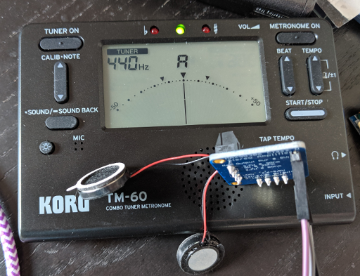
An A4 note played on an Adafruit MAX98306 audio amplifier board. The STM32F303 is not pictured, but I used a ‘Nucleo-32’ board.
Cool! But the signal is less stable over time than it looks in that picture, and in this example the right speaker is silent. The same logic works with DAC1 / Channel 2, DMA1 / Channel 4, pin A5, and (for example) the TIM7 timer, though. So can you make a 440Hz A4 play on the left speaker while a 294Hz D4 note plays on the right?
I’m sure you can! Now let’s move on and use the same example to learn how the other types of STM32 DMA peripherals work.
Part 2: F2/F4/F7 and G0/G4/L4+ DMA
Next, let’s look at the ‘Type 2’ DMA peripherals used in the higher-speed F2, F4, and F7 lines and the ‘Type 3’ DMA peripherals used in the newer G0, G4, and L4R / L4S lines. The ‘Type 2’ DMAs include two ‘source’ address registers intended for double-buffering, and the ‘Type 3’ DMAs include an extra ‘DMA multiplexer’ peripheral which lets you choose which peripherals map to which DMA channels.
Generating an Audio Tone with an F2/F4/F7 DMA Peripheral
I’ll use an STM32F413 ‘Nucleo-144‘ board as an example to generate the same audio tone as above. The ‘Type 2’ DMA peripheral is almost identical to the ‘Type 1’ peripheral if we don’t enable double-buffering, which we won’t. But ST also added a little bit more flexibility in this DMA peripheral; you still can’t configure which peripherals map to which DMA channels, but you can choose from a few different options per channel.
Unfortunately, the naming conventions are a bit confusing. In these F2/F4/F7 lines, each DMA peripheral has up to 8 ‘streams’ which each receive signals from 1 of 16 ‘channels’. So what we called ‘channels’ in the previous example are now called ‘streams’, and ‘channel’ means something else. Sorry, but as an example of how it is more flexible than ‘Type 1’ DMA, we don’t need to use the SYSCFG peripheral to remap the DAC peripheral mapping like we did in the previous example. Instead of being a special case, that configuration is part of the usual DMA configuration process.
Anyways, here is the simple DMA/DAC example from above, adapted for the STM32F413:
// Standard library includes.
#include <stdint.h>
#include <stdlib.h>
// Vendor-provided device header file.
#include "stm32f4xx.h"

// 32-sample sine wave.
#define _AMP(x) ( x / 8 )
const size_t SINE_SAMPLES = 32;
const uint16_t SINE_WAVE[] = {
  _AMP(2048), _AMP(2447), _AMP(2831), _AMP(3185),
  _AMP(3495), _AMP(3750), _AMP(3939), _AMP(4056),
  _AMP(4095), _AMP(4056), _AMP(3939), _AMP(3750),
  _AMP(3495), _AMP(3185), _AMP(2831), _AMP(2447),
  _AMP(2048), _AMP(1649), _AMP(1265), _AMP(911),
  _AMP(601),  _AMP(346),  _AMP(157),  _AMP(40),
  _AMP(0),    _AMP(40),   _AMP(157),  _AMP(346),
  _AMP(601),  _AMP(911),  _AMP(1265), _AMP(1649)
};

// Global variable to hold the core clock speed in Hertz.
uint32_t SystemCoreClock = 16000000;

// Simple imprecise delay method.
void __attribute__( ( optimize( "O0" ) ) )
delay_cycles( uint32_t cyc ) {
  for ( uint32_t d_i = 0; d_i < cyc; ++d_i ) { asm( "NOP" ); }
}

/**
 * Main program.
 */
int main(void) {
  // Enable peripherals: GPIOA, DMA, DAC, TIM6.
  RCC->AHB1ENR  |= ( RCC_AHB1ENR_GPIOAEN |
                     RCC_AHB1ENR_DMA1EN );
  RCC->APB1ENR  |= ( RCC_APB1ENR_DACEN |
                     RCC_APB1ENR_TIM6EN );

  // Pin A4 output type: Analog.
  GPIOA->MODER    &= ~( 0x3 << ( 4 * 2 ) );
  GPIOA->MODER    |=  ( 0x3 << ( 4 * 2 ) );

  // DMA configuration (channel 7 / stream 5).
  // SxCR register:
  // - Memory-to-peripheral
  // - Circular mode enabled.
  // - Increment memory ptr, don't increment periph ptr.
  // - 16-bit data size for both source and destination.
  // - High priority (2/3).
  DMA1_Stream5->CR &= ~( DMA_SxCR_CHSEL |
                         DMA_SxCR_PL |
                         DMA_SxCR_MSIZE |
                         DMA_SxCR_PSIZE |
                         DMA_SxCR_PINC |
                         DMA_SxCR_EN );
  DMA1_Stream5->CR |=  ( ( 0x2 << DMA_SxCR_PL_Pos ) |
                         ( 0x1 << DMA_SxCR_MSIZE_Pos ) |
                         ( 0x1 << DMA_SxCR_PSIZE_Pos ) |
                         ( 0x7 << DMA_SxCR_CHSEL_Pos ) |
                         DMA_SxCR_MINC |
                         DMA_SxCR_CIRC |
                         ( 0x1 << DMA_SxCR_DIR_Pos ) );
  // Set DMA source and destination addresses.
  // Source: Address of the sine wave buffer in memory.
  DMA1_Stream5->M0AR  = ( uint32_t )&SINE_WAVE;
  // Dest.: DAC1 Ch1 '12-bit right-aligned data' register.
  DMA1_Stream5->PAR   = ( uint32_t )&( DAC1->DHR12R1 );
  // Set DMA data transfer length (# of sine wave samples).
  DMA1_Stream5->NDTR  = ( uint16_t )SINE_SAMPLES;
  // Enable DMA1 Stream 5.
  DMA1_Stream5->CR   |= ( DMA_SxCR_EN );

  // TIM6 configuration.
  // Set prescaler and autoreload for a 440Hz sine wave.
  TIM6->PSC  =  ( 0x0000 );
  TIM6->ARR  =  ( SystemCoreClock / ( 440 * SINE_SAMPLES ) );
  // Enable trigger output on timer update events.
  TIM6->CR2 &= ~( TIM_CR2_MMS );
  TIM6->CR2 |=  ( 0x2 << TIM_CR2_MMS_Pos );
  // Start the timer.
  TIM6->CR1 |=  ( TIM_CR1_CEN );

  // DAC configuration.
  // Set trigger sources to TIM6 TRGO.
  DAC1->CR  &= ~( DAC_CR_TSEL1 );
  // Enable DAC DMA requests.
  DAC1->CR  |=  ( DAC_CR_DMAEN1 );
  // Enable DAC Channels.
  DAC1->CR  |=  ( DAC_CR_EN1 );
  // Delay briefly to allow sampling to stabilize (?)
  delay_cycles( 1000 );
  // Enable DAC channel trigger.
  DAC1->CR  |=  ( DAC_CR_TEN1 );

  // Done; a low-res 440Hz sine wave should be playing on PA4.
  while (1) {}
}
The ‘Nucleo-144’ board maps PA4 to its SPI_B bus and it’s not clearly marked on the board, so here’s a picture of how I wired it. Again, this sort of information can be found in the board’s user manual:
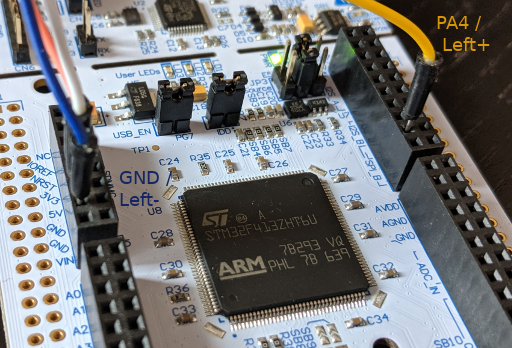
PA4 DAC pin on an STM32F413ZH Nucleo-144 board.
Generating an Audio Tone With a G0/G4/L4+ DMA Peripheral
Finally, I’ll use an STM32G071 ‘Nucleo-64‘ board to demonstrate how a ‘Type 3’ DMA peripheral works. The initialization is almost exactly the same as the simple ‘Type 1’ DMA, but there is an extra DMAMUX peripheral which explicitly maps a peripheral signal to a DMA channel. This is much more flexible than the configuration options that we saw in the ‘Type 2’ DMA peripheral, because it lets you map any peripheral to any DMA channel. Here’s the code:
// Standard library includes.
#include <stdint.h>
#include <stdlib.h>
// Vendor-provided device header file.
#include "stm32g0xx.h"

// 32-sample sine wave.
#define _AMP(x) ( x / 8 )
const size_t SINE_SAMPLES = 32;
const uint16_t SINE_WAVE[] = {
  _AMP(2048), _AMP(2447), _AMP(2831), _AMP(3185),
  _AMP(3495), _AMP(3750), _AMP(3939), _AMP(4056),
  _AMP(4095), _AMP(4056), _AMP(3939), _AMP(3750),
  _AMP(3495), _AMP(3185), _AMP(2831), _AMP(2447),
  _AMP(2048), _AMP(1649), _AMP(1265), _AMP(911),
  _AMP(601),  _AMP(346),  _AMP(157),  _AMP(40),
  _AMP(0),    _AMP(40),   _AMP(157),  _AMP(346),
  _AMP(601),  _AMP(911),  _AMP(1265), _AMP(1649)
};

// Global variable to hold the core clock speed in Hertz.
uint32_t SystemCoreClock = 16000000;

// Simple imprecise delay method.
void __attribute__( ( optimize( "O0" ) ) )
delay_cycles( uint32_t cyc ) {
  for ( uint32_t d_i = 0; d_i < cyc; ++d_i ) { asm( "NOP" ); }
}

/**
 * Main program.
 */
int main(void) {
  // Enable peripherals: GPIOA, DMA, DAC, TIM6.
  RCC->IOPENR   |= RCC_IOPENR_GPIOAEN;
  RCC->AHBENR   |= RCC_AHBENR_DMA1EN;
  RCC->APBENR1  |= ( RCC_APBENR1_DAC1EN |
                     RCC_APBENR1_TIM6EN );

  // Pin A4 output type: Analog.
  GPIOA->MODER    &= ~( 0x3 << ( 4 * 2 ) );
  GPIOA->MODER    |=  ( 0x3 << ( 4 * 2 ) );

  // DMA configuration (channel 1).
  // CCR register:
  // - Memory-to-peripheral
  // - Circular mode enabled.
  // - Increment memory ptr, don't increment periph ptr.
  // - 16-bit data size for both source and destination.
  // - High priority.
  uint32_t dma_ccr_clr = ~( DMA_CCR_MEM2MEM |
                            DMA_CCR_PL |
                            DMA_CCR_MSIZE |
                            DMA_CCR_PSIZE |
                            DMA_CCR_PINC |
                            DMA_CCR_EN );
  uint32_t dma_ccr_set =  ( ( 0x2 << DMA_CCR_PL_Pos ) |
                            ( 0x1 << DMA_CCR_MSIZE_Pos ) |
                            ( 0x1 << DMA_CCR_PSIZE_Pos ) |
                            DMA_CCR_MINC |
                            DMA_CCR_CIRC |
                            DMA_CCR_DIR );
  DMA1_Channel1->CCR &= dma_ccr_clr;
  DMA1_Channel1->CCR |= dma_ccr_set;
  // Select DAC Ch1 as DMA Ch1 request source in DMAMUX.
  // Note: DMAMUX channel numbers are slightly confusing in
  // the documentation. They aren't reliably 0- or 1-indexed.
  DMAMUX1_Channel0->CCR &= ~( DMAMUX_CxCR_DMAREQ_ID );
  DMAMUX1_Channel0->CCR |=  ( 0x8 << DMAMUX_CxCR_DMAREQ_ID_Pos );
  // Set DMA source and destination addresses.
  // Source: Address of the sine wave buffer in memory.
  DMA1_Channel1->CMAR  = ( uint32_t )&SINE_WAVE;
  // Dest.: DAC1 Ch1 '12-bit right-aligned data' register.
  DMA1_Channel1->CPAR  = ( uint32_t )&( DAC1->DHR12R1 );
  // Set DMA data transfer length (# of sine wave samples).
  DMA1_Channel1->CNDTR = ( uint16_t )SINE_SAMPLES;
  // Enable DMA1 Channels 1/2.
  DMA1_Channel1->CCR |= ( DMA_CCR_EN );

  // TIM6 configuration.
  // Set prescaler and autoreload for a 440Hz sine wave.
  TIM6->PSC  =  ( 0x0000 );
  TIM6->ARR  =  ( SystemCoreClock / ( 440 * SINE_SAMPLES ) );
  // Enable trigger output on timer update events.
  TIM6->CR2 &= ~( TIM_CR2_MMS );
  TIM6->CR2 |=  ( 0x2 << TIM_CR2_MMS_Pos );
  // Start the timer.
  TIM6->CR1 |=  ( TIM_CR1_CEN );

  // DAC configuration.
  // Set trigger source to TIM6 TRGO.
  DAC1->CR  &= ~( DAC_CR_TSEL1 );
  DAC1->CR  |=  ( 0x5 << DAC_CR_TSEL1_Pos );
  // Set outputs to buffered GPIO 'normal mode'.
  DAC1->MCR &= ~( DAC_MCR_MODE1 );
  // Enable DAC DMA requests.
  DAC1->CR  |=  ( DAC_CR_DMAEN1 );
  // Enable DAC Channels.
  DAC1->CR  |=  ( DAC_CR_EN1 );
  // Delay briefly to allow sampling to stabilize (?)
  delay_cycles( 1000 );
  // Enable DAC channel trigger.
  DAC1->CR  |=  ( DAC_CR_TEN1 );

  // Done; a low-res 440Hz sine wave should be playing on PA4.
  while (1) {}
}
And on the ‘Nucleo-64‘ board, PA4 is marked ‘A2’ on the board’s silkscreen.
Troubleshooting DAC Transfers
Note that you might need to modify this code slightly depending on which sort of STM32 chip you’re using, or if you decide to use DMA interrupts in your code. A helpful reader reported in the comments that the DAC destination registers should be treated as 32-bit registers instead of 16-bit ones on STM32G4 chips, and possibly others as well. So if you have trouble getting interrupts working, or if you have issues where the TEIF “Transfer Error” flag gets set, try setting the DMA channel’s PSIZE field to 2 for a 32-bit destination instead of 1 for a 16-bit one. Thank you for the extra information, Dirk!
Part 3: Lights and Displays
Okay, now let’s get to the fun stuff. Everybody likes colorful lights and displays, and everybody likes to see them refresh quickly. We’ll start with using SPI to drive ‘NeoPixel’ LEDs, then we’ll use I2C to drive a small monochorme OLED and SPI to drive a larger color TFT display.
I’ll use a ‘Type-3’ DMA peripheral for these examples, but you should be able to adapt them to ‘Type-1’ and ‘Type-2’ peripherals by adjusting the DMA channel and/or stream number to match the peripheral being used. And I’m sorry that the SPI/I2C/RCC/etc. registers might not quite match up, but those differences shouldn’t be too hard to resolve by checking the register definitions in your reference manual. Please feel free to comment if you run into trouble.
Pretty Colors
While WS2812 and SK6812 LEDs are starting to give way to newer SPI/I2C LEDs like APA102s, they are still cheap and common. They require precise timings, but you can actually use a SPI peripheral to generate those timings if you have a convenient clock speed. The basic idea is that you send a byte like 0b11000000 (0xC0) for 0, and something like 0b11111100 (0xFC) for 1. If the baud rate is set correctly, you can make those bytes into close-enough ~333-nanosecond and ~999-nanosecond pulses to represent one bit in the ‘Neopixel’ interface.
So that’s what we’ll do, and then we’ll set up a circular DMA transfer from an array of colors which we will update in the program’s main loop. To follow along with this example, you’ll need at least one WS2812-type LED, but the smooth rainbow effect will be easier to see with more LEDs.
Conveniently, 333 nanoseconds is 4 ‘ticks’ at 12MHz and 1332 nanoseconds is 16. So at a modest 48MHz core clock speed, we can use a SPI prescaler of 8 to make one SPI byte equal to a full ‘pulse’ of ~1250 nanoseconds, which is one bit to the ‘NeoPixel’. I also added 64 empty bytes at the end of the array, to allow for the required 10-50 microsecond ‘latch’ period which locks the LED colors after they are all sent.
One caveat: this isn’t very efficient, because every bit of neopixel color requires an entire byte of memory. But this is just a demo:
// Standard library includes.
#include <stdint.h>
#include <stdlib.h>
// Vendor-provided device header file.
#include "stm32g0xx.h"

// Array of LED colors. G/R/B/G/R/B/...
#define NUM_LEDS  ( 90 )
#define LED_BYTES ( ( NUM_LEDS * 3 * 8 ) + 64 )
uint8_t COLORS[ LED_BYTES ];

// Global variable to hold the core clock speed in Hertz.
uint32_t SystemCoreClock = 16000000;

// Simple imprecise delay method.
void __attribute__( ( optimize( "O0" ) ) )
delay_cycles( uint32_t cyc ) {
  for ( uint32_t d_i = 0; d_i < cyc; ++d_i ) { asm( "NOP" ); }
}

// Get a 32-bit representation of R/G/B colors.
uint32_t get_rgb_color( uint8_t r, uint8_t g, uint8_t b ) {
  return ( g << 16 | r << 8 | b );
}

// Set an LED to an RGB color.
void set_color( size_t led_index, uint32_t col ) {
  size_t led_base = led_index * 24;
  uint8_t r = ( col >> 8 ) & 0xFF;
  uint8_t g = ( col >> 16 ) & 0xFF;
  uint8_t b = ( col ) & 0xFF;
  for ( size_t i = 0; i < 8; ++i ) {
    if ( g & ( 1 << ( 7 - i ) ) ) { COLORS[ i + led_base ] = 0xFC; }
    else { COLORS[ i + led_base ] = 0xC0; }
  }
  for ( size_t i = 0; i < 8; ++i ) {
    if ( r & ( 1 << ( 7 - i ) ) ) { COLORS[ i + led_base + 8 ] = 0xFC; }
    else { COLORS[ i + led_base + 8 ] = 0xC0; }
  }
  for ( size_t i = 0; i < 8; ++i ) {
    if ( b & ( 1 << ( 7 - i ) ) ) { COLORS[ i + led_base + 16 ] = 0xFC; }
    else { COLORS[ i + led_base + 16 ] = 0xC0; }
  }
}

// Get the red component of an LED color.
uint8_t get_led_r( size_t led_num ) {
  uint8_t r = 0x00;
  for ( size_t i = 0; i < 8; ++i ) {
    if ( COLORS[ ( led_num * 24 ) + 8 + i ] != 0xC0 ) {
      r = r | ( 1 << ( 7 - i ) );
    }
  }
  return r;
}

// Get the green component of an LED color.
uint8_t get_led_g( size_t led_num ) {
  uint8_t g = 0x00;
  for ( size_t i = 0; i < 8; ++i ) {
    if ( COLORS[ ( led_num * 24 ) + i ] != 0xC0 ) {
      g = g | ( 1 << ( 7 - i ) );
    }
  }
  return g;
}

// Get the blue component of an LED color.
uint8_t get_led_b( size_t led_num ) {
  uint8_t b = 0x00;
  for ( size_t i = 0; i < 8; ++i ) {
    if ( COLORS[ ( led_num * 24 ) + 16 + i ] != 0xC0 ) {
      b = b | ( 1 << ( 7 - i ) );
    }
  }
  return b;
}

// Max brightness (out of a possible 255)
#define MAX_B ( 63 )
// How quickly to increment/decrement the colors.
#define B_INC ( 1 )
// Cycle the array of colors through a rainbow.
// Red -> Purple -> Blue -> Teal -> Green -> Yellow -> Red
// - If red > 0 and < max, if blue is 0, add red.
// - If red is max and blue is < max, add blue.
// - If blue is max and red is > 0, remove red.
// - If blue is max and green < 0, add green.
// - If green is max and blue > 0, remove blue.
// - If green is max and red < 0, add red.
// - If red is max and green is > 0, remove green.
void rainbow( void ) {
  uint8_t r = get_led_r( 0 );
  uint8_t g = get_led_g( 0 );
  uint8_t b = get_led_b( 0 );
  for ( int i = 0; i < NUM_LEDS; ++i ) {
    if ( r == 0 && g == 0 && b == 0 ) { r = B_INC; }
    if ( r > 0 && r < MAX_B && b == 0 ) { r += B_INC; }
    else if ( r >= MAX_B && b < MAX_B && g == 0 ) { b += B_INC; }
    else if ( b >= MAX_B && r > 0 ) { r -= B_INC; }
    else if ( b >= MAX_B && g < MAX_B ) { g += B_INC; }
    else if ( g >= MAX_B && b > 0 ) { b -= B_INC; }
    else if ( g >= MAX_B && r < MAX_B ) { r += B_INC; }
    else if ( r >= MAX_B && g > 0 ) { g -= B_INC; }
    else { r = 0; g = 0; b = 0; }
    set_color( i, get_rgb_color( r, g, b ) );
  }
}

/**
 * Main program.
 */
int main(void) {
  // Set initial colors to 'off'.
  for ( size_t i = 0; i < NUM_LEDS; ++i ) {
    set_color( i, get_rgb_color( 0x00, 0x00, 0x00 ) );
  }
  // Set the latching period to all 0s.
  for ( size_t i = LED_BYTES - 64; i < LED_BYTES; ++i ) {
    COLORS[ i ] = 0x00;
  }
  // Enable peripherals: GPIOB, DMA, SPI1.
  RCC->IOPENR   |= RCC_IOPENR_GPIOBEN;
  RCC->AHBENR   |= RCC_AHBENR_DMA1EN;
  RCC->APBENR2  |= RCC_APBENR2_SPI1EN;

  // Setup core clock to 48MHz.
  // Set 2 wait states in Flash.
  FLASH->ACR &= ~( FLASH_ACR_LATENCY );
  FLASH->ACR |=  ( 2 << FLASH_ACR_LATENCY_Pos );
  // Configure PLL; R = 2, M = 1, N = 6.
  // freq = ( 16MHz * ( N / M ) ) / R
  RCC->PLLCFGR &= ~( RCC_PLLCFGR_PLLR |
                     RCC_PLLCFGR_PLLREN |
                     RCC_PLLCFGR_PLLN |
                     RCC_PLLCFGR_PLLM |
                     RCC_PLLCFGR_PLLSRC );
  RCC->PLLCFGR |=  ( 1 << RCC_PLLCFGR_PLLR_Pos |
                     6 << RCC_PLLCFGR_PLLN_Pos |
                     RCC_PLLCFGR_PLLREN |
                     2 << RCC_PLLCFGR_PLLSRC_Pos );
  // Enable and select the PLL.
  RCC->CR   |= RCC_CR_PLLON;
  while ( !( RCC->CR & RCC_CR_PLLRDY ) ) {};
  RCC->CFGR &= ~( RCC_CFGR_SW );
  RCC->CFGR |=  ( 2 << RCC_CFGR_SW_Pos );
  while ( ( RCC->CFGR & RCC_CFGR_SWS ) >> RCC_CFGR_SWS_Pos != 2 ) {};
  // System clock is now 48MHz.
  SystemCoreClock = 48000000;

  // Setup pin: just one for this demo, PB5 is AF#0 (SPI1 SDO).
  GPIOB->MODER    &= ~( 0x3 << ( 5 * 2 ) );
  GPIOB->MODER    |=  ( 0x2 << ( 5 * 2 ) );
  GPIOB->AFR[ 0 ] &= ~( GPIO_AFRL_AFSEL5 );

  // DMA configuration (channel 1).
  // CCR register:
  // - Memory-to-peripheral
  // - Circular mode enabled.
  // - Increment memory ptr, don't increment periph ptr.
  // - -bit data size for both source and destination.
  // - High priority.
  DMA1_Channel1->CCR &= ~( DMA_CCR_MEM2MEM |
                           DMA_CCR_PL |
                           DMA_CCR_MSIZE |
                           DMA_CCR_PSIZE |
                           DMA_CCR_PINC |
                           DMA_CCR_EN );
  DMA1_Channel1->CCR |=  ( ( 0x2 << DMA_CCR_PL_Pos ) |
                           DMA_CCR_MINC |
                           DMA_CCR_CIRC |
                           DMA_CCR_DIR );
  // Route DMA channel 0 to SPI1 transmit.
  DMAMUX1_Channel0->CCR &= ~( DMAMUX_CxCR_DMAREQ_ID );
  DMAMUX1_Channel0->CCR |=  ( 17 << DMAMUX_CxCR_DMAREQ_ID_Pos );
  // Set DMA source and destination addresses.
  // Source: Address of the framebuffer.
  DMA1_Channel1->CMAR  = ( uint32_t )&COLORS;
  // Destination: SPI1 data register.
  DMA1_Channel1->CPAR  = ( uint32_t )&( SPI1->DR );
  // Set DMA data transfer length (framebuffer length).
  DMA1_Channel1->CNDTR = ( uint16_t )LED_BYTES;

  // SPI1 configuration:
  // - Clock phase/polarity: 1/1
  // - Assert internal CS signal (software CS pin control)
  // - MSB-first
  // - 8-bit frames
  // - Baud rate prescaler of 8 (for a 6MHz bit-clock)
  // - TX DMA requests enabled.
  SPI1->CR1 &= ~( SPI_CR1_LSBFIRST |
                  SPI_CR1_BR );
  SPI1->CR1 |=  ( SPI_CR1_SSM |
                  SPI_CR1_SSI |
                  0x2 << SPI_CR1_BR_Pos |
                  SPI_CR1_MSTR |
                  SPI_CR1_CPOL |
                  SPI_CR1_CPHA );
  SPI1->CR2 &= ~( SPI_CR2_DS );
  SPI1->CR2 |=  ( 0x7 << SPI_CR2_DS_Pos |
                  SPI_CR2_TXDMAEN );
  // Enable the SPI peripheral.
  SPI1->CR1 |=  ( SPI_CR1_SPE );

  // Enable DMA1 Channel 1 to start sending colors.
  DMA1_Channel1->CCR |= ( DMA_CCR_EN );

  // Done; now just cycle between colors.
  while (1) {
    rainbow();
    delay_cycles( 10000 );
  }
}
Run that, connect a strand of compatible LEDs, and voila. A rainbow. Adjusting the number in the delay_cycles call will make the rainbow pulse more slowly or quickly:
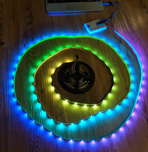
With DMA, you can easily hit the 800KHz maximum speed of the single-wire interface used by these LEDs.
I2C OLEDs
Next, let’s draw to some small I2C OLED displays, specifically monochrome 128×64 SSD1306 displays. These are nice cheap displays for small projects, and you’ll need one to follow along with this example.
This application uses the same basic idea as the last one, just with I2C and a different sort of framebuffer. But unlike with SPI, the STM32’s I2C peripheral requires us to define how many bytes we want to send before we start transmitting. That means that we can’t ‘set and forget’ a DMA channel, because the I2C peripheral will stop sending DMA requests once its counter reaches zero. But hey, that’ll give us an opportunity to learn how to use interrupts to manage DMA flow when necessary.
Specifically, we can use the I2C peripheral’s “transfer complete” interrupt to reset the ‘number of bytes’ counter when it reaches zero. We can also use a single non-circular DMA transfer to send the required initialization commands before we start drawing to the display. Here’s the code:
// Standard library includes.
#include <stdint.h>
#include <stdlib.h>
// Vendor-provided device header file.
#include "stm32g0xx.h"

// 128x64-pixel monochrome framebuffer.
#define SSD1306_W 128
#define SSD1306_H 64
#define SSD1306_A ( SSD1306_W * SSD1306_H ) / 8
uint8_t FRAMEBUFFER[ SSD1306_A ];
// Initialization commands for the SSD1306 display.
#define NUM_INIT_CMDS 25
const uint8_t INIT_CMDS[ NUM_INIT_CMDS ] = {
  // 0x00, to indicate command bytes.
  0x00,
  // Display clock division, multiplex (# rows)
  0xD5, 0x80, 0xA8, 0x3F,
  // Display offset, start line, charge pump on.
  0xD3, 0x00, 0x40, 0x8D, 0x14,
  // Memory mode, segment remap, desc. column scan.
  0x20, 0x00, 0xA1, 0xC8,
  // 'COMPINS', contrast.
  0xDA, 0x12, 0x81, 0x0A,
  // precharge, VCOM detection level.
  0xD9, 0xF1, 0xDB, 0x40,
  // Output follows RAM, normal mode, display on.
  0xA4, 0xA6, 0xAF
};

// Global variable to hold the core clock speed in Hertz.
uint32_t SystemCoreClock = 16000000;

// Simple imprecise delay method.
void __attribute__( ( optimize( "O0" ) ) )
delay_cycles( uint32_t cyc ) {
  for ( uint32_t d_i = 0; d_i < cyc; ++d_i ) { asm( "NOP" ); }
}

/**
 * Main program.
 */
int main(void) {
  // Enable peripherals: GPIOA, DMA, I2C2.
  RCC->IOPENR   |= RCC_IOPENR_GPIOAEN;
  RCC->AHBENR   |= RCC_AHBENR_DMA1EN;
  RCC->APBENR1  |= RCC_APBENR1_I2C2EN;

  // Pin A11/12 output type: Alt. Func. #6.
  GPIOA->MODER    &= ~( 0x3 << ( 11 * 2 ) |
                        0x3 << ( 12 * 2 ) );
  GPIOA->MODER    |=  ( 0x2 << ( 11 * 2 ) |
                        0x2 << ( 12 * 2 ) );
  GPIOA->AFR[ 1 ] &= ~( GPIO_AFRH_AFSEL11 |
                        GPIO_AFRH_AFSEL12 );
  GPIOA->AFR[ 1 ] |=  ( 0x6 << GPIO_AFRH_AFSEL11_Pos |
                        0x6 << GPIO_AFRH_AFSEL12_Pos );

  // DMA configuration (channel 1).
  // CCR register:
  // - Memory-to-peripheral
  // - Circular mode disabled.
  // - Increment memory ptr, don't increment periph ptr.
  // - 8-bit data size for both source and destination.
  // - High priority.
  DMA1_Channel1->CCR &= ~( DMA_CCR_MEM2MEM |
                           DMA_CCR_PL |
                           DMA_CCR_MSIZE |
                           DMA_CCR_PSIZE |
                           DMA_CCR_PINC |
                           DMA_CCR_CIRC |
                           DMA_CCR_EN );
  DMA1_Channel1->CCR |=  ( ( 0x2 << DMA_CCR_PL_Pos ) |
                           DMA_CCR_MINC |
                           DMA_CCR_DIR );
  // Route DMA channel 0 to I2C2 transmit.
  DMAMUX1_Channel0->CCR &= ~( DMAMUX_CxCR_DMAREQ_ID );
  DMAMUX1_Channel0->CCR |=  ( 13 << DMAMUX_CxCR_DMAREQ_ID_Pos );
  // Set DMA source and destination addresses.
  // Source: Address of the initialization commands.
  DMA1_Channel1->CMAR  = ( uint32_t )&INIT_CMDS;
  // Dest.: 'I2C2 transmit' register.
  DMA1_Channel1->CPAR  = ( uint32_t )&( I2C2->TXDR );
  // Set DMA data transfer length (# of init commands).
  DMA1_Channel1->CNDTR = ( uint16_t )NUM_INIT_CMDS;
  // Enable DMA1 Channel 1.
  DMA1_Channel1->CCR |= ( DMA_CCR_EN );

  // I2C2 configuration:
  // Timing register. For "Fast-Mode+" (1MHz), the RM says:
  // (@16MHz) presc=0, SCLL=4, SCLH=2, SDADEL=0, SCLDEL=2.
  I2C2->TIMINGR  = 0x00200204;
  // Enable the peripheral.
  I2C2->CR1     |= I2C_CR1_PE;
  // Set the device address. Usually 0x78, can be 0x7A.
  // The I2C peripheral also needs to know how many bytes
  // to send before it starts transmitting.
  I2C2->CR2     &= ~( I2C_CR2_SADD |
                      I2C_CR2_NBYTES );
  I2C2->CR2     |=  ( 0x78 << I2C_CR2_SADD_Pos |
                      NUM_INIT_CMDS << I2C_CR2_NBYTES_Pos );
  // Enable I2C DMA requests.
  I2C2->CR1     |=  ( I2C_CR1_TXDMAEN );
  // Send a start signal.
  I2C2->CR2     |=  ( I2C_CR2_START );
  // (DMA is now running.)
  // Wait for DMA to finish.
  while ( !( DMA1->ISR & DMA_ISR_TCIF1 ) ) {};
  DMA1->IFCR |= DMA_IFCR_CTCIF1;
  // Stop the I2C transmission.
  while ( !( I2C2->ISR & I2C_ISR_TC ) ) {};
  I2C2->CR2  |=  ( I2C_CR2_STOP );
  while ( I2C2->ISR & I2C_ISR_BUSY ) {};

  // Reconfigure DMA and I2C for sending the framebuffer.
  // Disable the DMA channel.
  DMA1_Channel1->CCR &= ~( DMA_CCR_EN );
  // Set DMA circular mode.
  DMA1_Channel1->CCR |=  ( DMA_CCR_CIRC );
  // Set I2C autoreload and the maximum 255 byte length.
  I2C2->CR2      &= ~( I2C_CR2_NBYTES );
  I2C2->CR2      |=  ( I2C_CR2_RELOAD |
                       255 << I2C_CR2_NBYTES_Pos );
  // Enable the I2C2 interrupt.
  NVIC_SetPriority( I2C2_IRQn, 0x03 );
  NVIC_EnableIRQ( I2C2_IRQn );
  // Enable the 'transfer complete' I2C interrupt.
  I2C2->CR1      |= I2C_CR1_TCIE;
  // Update DMA source/destination/size registers.
  // Source: Address of the framebuffer.
  DMA1_Channel1->CMAR  = ( uint32_t )&FRAMEBUFFER;
  // Dest.: 'I2C2 transmit' register.
  DMA1_Channel1->CPAR  = ( uint32_t )&( I2C2->TXDR );
  // Set DMA data transfer length (framebuffer length).
  DMA1_Channel1->CNDTR = ( uint16_t )SSD1306_A;
  // Send a start signal.
  I2C2->CR2     |=  ( I2C_CR2_START );
  while ( !( I2C2->CR2 & I2C_CR2_START ) ) {};
  // Send '0x40' to indicate display data.
  I2C2->TXDR = 0x40;
  // Re-enable DMA1 Channel 1.
  DMA1_Channel1->CCR |= ( DMA_CCR_EN );

  // Done; now draw patterns to the framebuffer.
  // The display is configured to hold 8 vertical pixels in
  // each byte, with the first 128 bytes representing
  // y-coordinates [0:7], the next 128 bytes [8:15], and so on.
  // So if we set each byte to the same value, it will look
  // like a pattern of horizontal lines of varying thickness.
  uint8_t val = 0x00;
  while (1) {
    // Draw the new pattern to the framebuffer.
    for ( size_t i = 0; i < SSD1306_A; ++i ) {
      FRAMEBUFFER[ i ] = val;
    }
    // Update the pattern.
    ++val;
    // Delay briefly.
    delay_cycles( 200000 );
  }
}

// I2C2 interrupt handler.
void I2C2_IRQ_handler( void ) {
  if ( I2C2->ISR & I2C_ISR_TCR ) {
    // Reset the 'number of bytes' counter.
    I2C2->CR2 &= ~( I2C_CR2_NBYTES );
    I2C2->CR2 |=  ( 255 << I2C_CR2_NBYTES_Pos );
  }
}
This I2C interrupt handler follows a pretty standard pattern:
Connect a display to the I2C pins, and it should light up very quickly. If it doesn’t, try using the alternate I2C address of 0x7A instead of 0x78:
Great, a pattern of horizontal lines. I’m sure you can find more exciting things to display 🙂
SPI TFTs
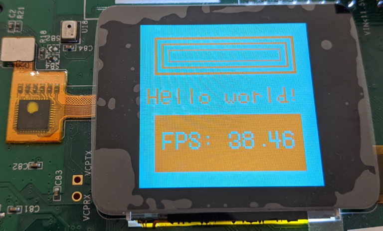
Finally, let’s look at some popular SPI TFT displays. The ILI9163C and ILI9341 controllers are used in many affordable display modules. Usually ILI9341 displays have a resolution of 240×320 and ILI9163C displays are 128×128 or 128×160, but there are exceptions.
And while most of the example code that you’ll see online includes dozens of initialization commands, you really only need a few commands, and those few essential commands seem to be shared between ILI9163C and ILI9341 displays. You can even connect them in parallel:
I can’t imagine why you would ever need to do this, but…it works.
But sadly, unlike the I2C display, we can’t send all of the initialization commands in a single DMA burst. These TFT displays’ “4-wire SPI” modes expect a “Data / Command” selection pin to be toggled between a command and the configuration data which follows. But once we’ve finished initializing the display, we can set up an ordinary circular DMA transfer to send the framebuffer:
// Standard library includes.
#include <stdint.h>
#include <stdlib.h>
// Vendor-provided device header file.
#include "stm32g0xx.h"

// 128x128-pixel 16-bit (RGB-565) framebuffer.
#define ILI9163C_W ( 128 )
#define ILI9163C_H ( 128 )
#define ILI9163C_A ( ILI9163C_W * ILI9163C_H )
uint16_t FRAMEBUFFER[ ILI9163C_A ];
// Macro definitions for 'command' (0) and 'data' (1) modes.
#define ILI9163C_CMD ( 0 )
#define ILI9163C_DAT ( 1 )
// Software-controlled pin macros, for convenience.
// B4 = CS, B6 = Reset, B7 = Data/Command.
#define TFT_CS  ( GPIO_ODR_OD4 )
#define TFT_RST ( GPIO_ODR_OD6 )
#define TFT_DC  ( GPIO_ODR_OD7 )

// Global variable to hold the core clock speed in Hertz.
uint32_t SystemCoreClock = 16000000;

// Simple imprecise delay method.
void __attribute__( ( optimize( "O0" ) ) )
delay_cycles( uint32_t cyc ) {
  for ( uint32_t d_i = 0; d_i < cyc; ++d_i ) { asm( "NOP" ); }
}

// Write a byte to the SPI peripheral.
void spi_w8( SPI_TypeDef *SPIx, uint8_t dat ) {
  // Wait for TXE 'transmit buffer empty' bit to be set.
  while ( !( SPIx->SR & SPI_SR_TXE ) ) {};
  // Send the byte.
  *( uint8_t* )&( SPIx->DR ) = dat;
}

// Write two bytes to the SPI peripheral. Note that they
// send in the order of 0x2211. (1 = first, 2 = second)
void spi_w16( SPI_TypeDef *SPIx, uint16_t dat ) {
  // Wait for TXE 'transmit buffer empty' bit to be set.
  while ( !( SPIx->SR & SPI_SR_TXE ) ) {};
  // Send the bytes.
  *( uint16_t* )&( SPIx->DR ) = dat;
}

// Method to set the 'data / command' pin.
void dat_cmd( SPI_TypeDef *SPIx, uint8_t dc ) {
  // Wait for the BSY 'busy' bit to be cleared.
  while ( SPIx->SR & SPI_SR_BSY ) {};
  // Set the D/C pin appropriately.
  if ( dc ) { GPIOB->ODR |=  ( TFT_DC ); }
  else      { GPIOB->ODR &= ~( TFT_DC ); }
}

/**
 * Main program.
 */
int main(void) {
  // Enable peripherals: GPIOB, DMA, SPI1.
  RCC->IOPENR   |= RCC_IOPENR_GPIOBEN;
  RCC->AHBENR   |= RCC_AHBENR_DMA1EN;
  RCC->APBENR2  |= RCC_APBENR2_SPI1EN;

  // Setup core clock to 64MHz.
  // Set 2 wait states in Flash.
  FLASH->ACR &= ~( FLASH_ACR_LATENCY );
  FLASH->ACR |=  ( 2 << FLASH_ACR_LATENCY_Pos );
  // Configure PLL; R = 2, M = 1, N = 8.
  // freq = ( 16MHz * ( N / M ) ) / R
  RCC->PLLCFGR &= ~( RCC_PLLCFGR_PLLR |
                     RCC_PLLCFGR_PLLREN |
                     RCC_PLLCFGR_PLLN |
                     RCC_PLLCFGR_PLLM |
                     RCC_PLLCFGR_PLLSRC );
  RCC->PLLCFGR |=  ( 1 << RCC_PLLCFGR_PLLR_Pos |
                     8 << RCC_PLLCFGR_PLLN_Pos |
                     RCC_PLLCFGR_PLLREN |
                     2 << RCC_PLLCFGR_PLLSRC_Pos );
  // Enable and select the PLL.
  RCC->CR   |= RCC_CR_PLLON;
  while ( !( RCC->CR & RCC_CR_PLLRDY ) ) {};
  RCC->CFGR &= ~( RCC_CFGR_SW );
  RCC->CFGR |=  ( 2 << RCC_CFGR_SW_Pos );
  while ( ( RCC->CFGR & RCC_CFGR_SWS ) >> RCC_CFGR_SWS_Pos != 2 ) {};
  // System clock is now 64MHz.
  SystemCoreClock = 64000000;

  // Setup pins: B3/5 are AF#0 (SPI1) (SCK/SDO),
  // B4 = CS, B6 = Reset, B7 = D/C.
  GPIOB->MODER    &= ~( 0x3 << ( 3 * 2 ) |
                        0x3 << ( 4 * 2 ) |
                        0x3 << ( 5 * 2 ) |
                        0x3 << ( 6 * 2 ) |
                        0x3 << ( 7 * 2 ) );
  GPIOB->MODER    |=  ( 0x2 << ( 3 * 2 ) |
                        0x1 << ( 4 * 2 ) |
                        0x2 << ( 5 * 2 ) |
                        0x1 << ( 6 * 2 ) |
                        0x1 << ( 7 * 2 ) );
  GPIOB->AFR[ 0 ] &= ~( GPIO_AFRL_AFSEL3 |
                        GPIO_AFRL_AFSEL5 );
  // Initial pin states: DC low, CS/Reset high.
  GPIOB->ODR      &= ~( TFT_DC );
  GPIOB->ODR      |=  ( TFT_CS | TFT_RST );

  // DMA configuration (channel 1).
  // CCR register:
  // - Memory-to-peripheral
  // - Circular mode enabled.
  // - Increment memory ptr, don't increment periph ptr.
  // - 16-bit data size for both source and destination.
  // - High priority.
  DMA1_Channel1->CCR &= ~( DMA_CCR_MEM2MEM |
                           DMA_CCR_PL |
                           DMA_CCR_MSIZE |
                           DMA_CCR_PSIZE |
                           DMA_CCR_PINC |
                           DMA_CCR_EN );
  DMA1_Channel1->CCR |=  ( ( 0x2 << DMA_CCR_PL_Pos ) |
                           ( 0x1 << DMA_CCR_MSIZE_Pos ) |
                           ( 0x1 << DMA_CCR_PSIZE_Pos ) |
                           DMA_CCR_MINC |
                           DMA_CCR_CIRC |
                           DMA_CCR_DIR );
  // Route DMA channel 0 to SPI1 transmit.
  DMAMUX1_Channel0->CCR &= ~( DMAMUX_CxCR_DMAREQ_ID );
  DMAMUX1_Channel0->CCR |=  ( 17 << DMAMUX_CxCR_DMAREQ_ID_Pos );
  // Set DMA source and destination addresses.
  // Source: Address of the framebuffer.
  DMA1_Channel1->CMAR  = ( uint32_t )&FRAMEBUFFER;
  // Destination: SPI1 data register.
  DMA1_Channel1->CPAR  = ( uint32_t )&( SPI1->DR );
  // Set DMA data transfer length (framebuffer length).
  DMA1_Channel1->CNDTR = ( uint16_t )ILI9163C_A;

  // Toggle pin B6 to reset the display.
  GPIOB->ODR &= ~( TFT_RST );
  delay_cycles( 200000 );
  GPIOB->ODR |=  ( TFT_RST );

  // SPI1 configuration:
  // - Clock phase/polarity: 1/1
  // - Assert internal CS signal (software CS pin control)
  // - MSB-first
  // - 8-bit frames
  // - Baud rate prescaler of 4 (or 128 for debugging)
  // - TX DMA requests enabled.
  SPI1->CR1 &= ~( SPI_CR1_LSBFIRST |
                  SPI_CR1_BR );
  SPI1->CR1 |=  ( SPI_CR1_SSM |
                  SPI_CR1_SSI |
                  0x1 << SPI_CR1_BR_Pos |
                  SPI_CR1_MSTR |
                  SPI_CR1_CPOL |
                  SPI_CR1_CPHA );
  SPI1->CR2 &= ~( SPI_CR2_DS );
  SPI1->CR2 |=  ( 0x7 << SPI_CR2_DS_Pos |
                  SPI_CR2_TXDMAEN );
  // Enable the SPI peripheral.
  SPI1->CR1 |=  ( SPI_CR1_SPE );

  // Send initialization commands.
  // Pull CS pin low.
  GPIOB->ODR &= ~( TFT_CS );
  // Software reset.
  dat_cmd( SPI1, ILI9163C_CMD );
  spi_w8( SPI1, 0x01 );
  delay_cycles( 200000 );
  // Display off.
  spi_w8( SPI1, 0x28 );
  // Color mode: 16bpp.
  spi_w8( SPI1, 0x3A );
  dat_cmd( SPI1, ILI9163C_DAT );
  spi_w8( SPI1, 0x55 );
  // Exit sleep mode.
  dat_cmd( SPI1, ILI9163C_CMD );
  spi_w8( SPI1, 0x11 );
  delay_cycles( 200000 );
  // Display on.
  spi_w8( SPI1, 0x29 );
  delay_cycles( 200000 );
  // Set drawing window.
  // The displays I got are offset by a few pixels.
  // So instead of setting X/Y ranges of [0:127]...
  // Column set: [2:129]
  spi_w8( SPI1, 0x2A );
  dat_cmd( SPI1, ILI9163C_DAT );
  spi_w16( SPI1, 0x0200 );
  spi_w16( SPI1, 0x8100 );
  dat_cmd( SPI1, ILI9163C_CMD );
  // Row set: [1:128]
  spi_w8( SPI1, 0x2B );
  dat_cmd( SPI1, ILI9163C_DAT );
  spi_w16( SPI1, 0x0100 );
  spi_w16( SPI1, 0x8000 );
  dat_cmd( SPI1, ILI9163C_CMD );
  // Set 'write to RAM' mode.
  spi_w8( SPI1, 0x2C );
  // From now on, we'll only be sending pixel data.
  dat_cmd( SPI1, ILI9163C_DAT );

  // Enable DMA1 Channel 1 to start sending the framebuffer.
  DMA1_Channel1->CCR |= ( DMA_CCR_EN );

  // Done; now just alternate between solid colors to get
  // a feel for the refresh speed.
  uint16_t color = 0x1984;
  while (1) {
    // Draw the new color to the framebuffer.
    for ( size_t i = 0; i < ILI9163C_A; ++i ) {
      FRAMEBUFFER[ i ] = color;
    }
    // Invert the color.
    color = color ^ 0xFFFF;
    // Delay briefly.
    delay_cycles( 2500000 );
  }
}
If you connect the TFT to the appropriate pins and run that code, it should flash between purple and teal colors. It does require a whopping 32KB of RAM, and even in an 8-bit color mode, a 240×320 ILI9341 display will require at least 75KB of RAM. That’s more than most MCUs have on-board, but that’s a problem for another day.
Conclusions
So there we go – a basic introduction to STM32 DMA peripherals. I hope this was helpful, and as usual corrections and comments are always appreciated. You can find example projects with the code shown in these examples in this GitHub repository.
This should help to demonstrate why DMA is useful, if you’ve been following along with any of my previous tutorials. The OLED and TFT display demos are noticeably faster than the previous examples which used polling to wait until the peripheral was ready to receive each byte. DMA is faster and more power-efficient if your application can sleep when it is idle, so it’s a good choice for a wide variety of applications.
I didn’t cover receiving data with DMA, but this post was getting sort of long. Still, you can reverse the direction and DMA is also great for something like filling a ring buffer when you are listening on a UART connection. That might be a good exercise for the reader 🙂
nucleo_user
November 26, 2019 at 8:26 am
Hi
Thats by far one of the best tutorials that I’ve ever read over DMA on STM32!
I would like to implement the exact same behaviour on my Nucleo-G474RE as you have implemented. For that I’ve changed the following lines:
DAC1->CR to 0x6
DMAMUX1_Channel0->CCR = 0x6
based on the reference manual.What else I’m missing? I always receive a DMA Transfer Error Irq and i don’t know why…
Vivonomicon
December 4, 2019 at 6:15 am
Hi, thank you for the kind words! I haven’t actually had the chance to test this with an STM32G4 nucleo board yet, so I could be wrong, but have you tried using 0x7 for the DAC1 trigger selection field? (Along with the other ‘enable’ / etc bits). It looks like dac_chx_trg7 might map to the TIM6_TRGO output, and a value of 0 in the TSEL bits maps to a software trigger so that a value of 0xN = dac_chx_trgN.
I hope that helps – and good luck with your projects!
nucleo_user
December 4, 2019 at 7:10 am
My fault. I found the problem… in the reference manuel chapter 21.7:
“The peripheral registers have to be accessed by words (32-bit).”
so I’ve configured the dma as word aligned.
Vivonomicon
February 11, 2020 at 3:56 pm
Oh, interesting – well congrats, I’m glad that you were able to get it working!
Victor Tagayun
June 21, 2020 at 4:26 pm
Sorry newbie here.
I cannot start any project in STM32 without using CubeMX, so bare metal is quite hard for me.
That also means that mostly it’s either I will be using HAL or LL.
My question is, how do you get to know the numerical values of the following codes?
DMA1_Stream5->CR |= ( ( 0x2 << DMA_SxCR_PL_Pos ) |
( 0x1 << DMA_SxCR_MSIZE_Pos ) |
( 0x1 << DMA_SxCR_PSIZE_Pos ) |
( 0x7 << DMA_SxCR_CHSEL_Pos )
ie, 0x2, 0x1 and 0x7. I assume those *_Pos are the bit positions in that particular registers and shifted according to their positions. But what number to write is quite confusing for me at the moment.
Vivonomicon
June 23, 2020 at 12:25 pm
You can find more information about peripheral register bitfields in the reference manual; each peripheral’s chapter has a “ Registers” section at the end. In this case, you can look under the “DMA stream x configuration register (DMA_SxCR)” subsection.
If you look at the “PL” bits (16:17), you can see that those represent priority levels; a higher number means a higher priority.
The “MSIZE” and “PSIZE” bits set the transfer size for the “memory” and “peripheral” sides; a value of 1 configures the stream for 16-bit transfers on both ends. (0 = 8-bit, 1 = 16-bit, 2 = 32-bit, 3 = reserved)
The “CHSEL” field holds “channel selection” bits, which determine which channel the DMA stream should be connected to. You can find peripheral : channel mappings in the “DMA” chapter of the reference manual, in the “Summary of DMA requests for each channel” table.
Sorry if the numbers were confusing; sometimes the device header files have named values for different bitfield settings, but it can also be easy to use numbers for things like priority levels or channel numbers when the values map neatly (like here, where 0x7 = channel #7). Maybe it’s a little bit lazy, but…oh well.
Dirk Handzic
July 9, 2020 at 1:04 am
Really a very useful tutorial about the different DMA types!
On a STM32G431 I am trying to use DMA to generate 2 DAC outputs, but somehow it does not work. I can see the counter is active DMA1 and DMAMUX are active but the DAC output changes only after the first load with 0x0fff. I can not see what I have missed:
// DMA setup output 1
DMA1_Channel2->CCR = (DMA_CCR_PL_1 | DMA_CCR_MINC | DMA_CCR_PSIZE_0 | DMA_CCR_MSIZE_0 | DMA_CCR_CIRC | DMA_CCR_DIR); // memory to peripheral, 16 bit aligned, transfer complete
DMA1_Channel2->CNDTR = SAMPLE_SIZE;
DMA1_Channel2->CPAR = (ULONG) &DAC1->DHR12R1;
DMA1_Channel2->CMAR = (ULONG)((UINT *)sample_buffer1); // Left channel 12 bit MSB
DMA1_Channel2->CCR |= DMA_CCR_HTIE | DMA_CCR_TCIE | DMA_CCR_TEIE;
DMAMUX1_Channel1->CCR = (0x06 <CFR = DMAMUX_CFR_CSOF1;
NVIC_SetPriority(DMA1_Channel5_IRQn, DMA_PRIO);
NVIC_EnableIRQ(DMA1_Channel2_IRQn);
DMA1_Channel2->CCR |= DMA_CCR_EN;
// DMA setup output 2
DMA1_Channel3->CCR = (DMA_CCR_PL_1 | DMA_CCR_MINC | DMA_CCR_PSIZE_0 | DMA_CCR_MSIZE_0 | DMA_CCR_CIRC | DMA_CCR_DIR ); // memory to peripheral, 16 bit aligned, transfer complete
DMA1_Channel3->CNDTR = SAMPLE_SIZE;
DMA1_Channel3->CPAR = (ULONG) &DAC1->DHR12R2;
DMA1_Channel3->CMAR = (ULONG)((UINT *)sample_buffer1 + 4); // Right channel 12 bit MSB
DMA1_Channel3->CCR |= DMA_CCR_HTIE | DMA_CCR_TCIE | DMA_CCR_TEIE;
DMAMUX1_Channel2->CCR = (0x07 <CFR = DMAMUX_CFR_CSOF2;
NVIC_SetPriority(DMA1_Channel3_IRQn, DMA_PRIO);
NVIC_EnableIRQ(DMA1_Channel3_IRQn);
DMA1_Channel3->CCR |= DMA_CCR_EN;
// DAC output trigger
TIM6->PSC = 0; // Timer clock
TIM6->ARR = (FOSC/(44100)); // Auto reload
TIM6->CR2 &= ~(TIM_CR2_MMS);
TIM6->CR2 |= (0x02 <CR1 |= TIM_CR1_CEN; // Start timer
//DAC output
DAC1->CR &= ~(DAC_CR_TEN1 | DAC_CR_TEN2 | DAC_CR_TSEL1 | DAC_CR_TSEL2 | DAC_CR_EN1 | DAC_CR_EN2);
DAC1->MCR &= ~(DAC_MCR_MODE1 | DAC_MCR_MODE2); // External buffered output
DAC1->CR |= (0x07 << DAC_CR_TSEL1_Pos) | (0x07 <CR |= DAC_CR_DMAEN1 | DAC_CR_DMAEN2;
DAC1->CR |= DAC_CR_EN1 | DAC_CR_EN2;
DAC1->CR |= DAC_CR_TEN1 | DAC_CR_TEN2;
DAC1->DHR12R1 = 0x0FFF;
DAC1->DHR12R2 = 0x0FFF;
Vivonomicon
July 26, 2020 at 1:56 pm
It looks like there might be some copy/paste typos there – like, this line doesn’t look valid:
DMAMUX1_Channel2->CCR = (0x07But assuming the syntax is right and some bits are missing in what you pasted, it looks like you might be setting the DMAMUX triggers to different values for each DAC channel? It looks like both DMAMUX CCR registers should use a request ID of 8 for TIM6 on an STM32G431. The ID and channel values seem like they might vary from chip to chip, so be sure to double-check those in the reference manual.
It's also possible that the HTIE, TEIE, or TCIE interrupts are halting or pausing the DMA transfer. Sometimes if you enable an interrupt and don't clear the appropriate "pending interrupt" flag after it triggers, the peripheral will stop to wait for you to acknowledge the interrupt.
Good luck!
Dirk
July 27, 2020 at 12:52 am
TIM6 is only generating the trigger for the DAC output. The reason why it has not been working is the data width of the DAC data register which has to be addressed as 32 bit even though it is only a 12 bit DAC. PSIZE in the DMA1_Channelx->CCR has to be set accordingly.
Vivonomicon
July 27, 2020 at 12:37 pm
Oh, interesting – so the PSIZE field should be set for 32 bits instead of 16 when DMA targets the DAC peripheral? Can you keep using a 16-bit MSIZE, or do you also have to change the source data to fit a 32-bit transfer?
I hadn’t realized that that could be an issue. Thank you for pointing it out!
Dirk
July 27, 2020 at 11:21 pm
Yes, MSIZE is still 16 bit wide but PSIZE needs to be 32 bit wide for STM32G431 DAC DMA access. Otherwise the TEIF indicates a transmission error.
Actually STM32CubeMX generates wrong code for DAC DMA access too 🙂 – which is not uncommon..
Vivonomicon
July 28, 2020 at 8:56 am
Ah, you learn something new every day. I’ll add a note to the end of the DAC sections mentioning that, thank you for the tip!
abadialali
August 13, 2020 at 10:06 pm
Hi there,
I am new to STM32 programing and I am interested in using the DMA with the DAC for the Arduino Portenta H7 which uses the STM32H747.
I was wondering if your code works and what type of changes I should look into.
Thanks
Vivonomicon
August 15, 2020 at 9:34 am
Hi, sorry that I didn’t include STM32H7 chips in this post. I don’t have a board with one handy, but it looks like their DMA peripherals are very similar to the “Type 3” ones from this post. They do have an extra “Basic DMA” peripheral though, so there might also be some extra features in the main DMAs.
Good luck!
Abdulwadood Al-Ali
August 15, 2020 at 7:44 pm
so that means I should be able to use your code for the type 3 for it. Thanks I will try it and let you know if I got it to work. Any specific things I should look into and change in the code?
Vivonomicon
August 16, 2020 at 2:42 pm
Not that I can think of off the top of my head, but it would be a good idea to check the “DMA” and “DMAMUX” chapters in your chip’s reference manual. If you look in the “Registers” sections at the end of the chapters, you can verify that the bit settings are in the same places. You might also need to use slightly different names for the registers and settings, depending on how they are defined in the “stm32h7[…].h” device header files.
And if you want to build the code using GCC and Makefiles like in the example projects I linked to, you’ll also need to modify the build system (Makefile, linker script, vector table). I think you can probably target a Cortex-M7 chip with the appropriate “STM32H7xx” flags, again defined in ST’s “stm32h7[…].h” device header files.
Good luck!